Philips pu17310 DATASHEETS

Philips Semiconductors Programmable Logic Devices Product specification
PLUS173–10
Programmable logic array
(22 × 42 × 10)
41
October 22, 1993 853–1422 11164
DESCRIPTION
The PLUS173–10 PLD is a high speed,
combinatorial Programmable Logic Array.
The Philips Semiconductors state-of-the-art
Oxide Isolated Bipolar fabrication process is
employed to produce maximum propagation
delays of 10ns or less.
The 24-pin PLUS173–10 device has a
programmable AND array and a
programmable OR array. Unlike PAL
devices, 100% product term sharing is
supported. Any of the 32 logic product terms
can be connected to any or all of the 10
output OR gates. Most PAL ICs are limited to
7 AND terms per OR function; the
PLUS173–10 device can support up to 32
input wide OR functions.
The polarity of each output is userprogrammable as either Active-High or
Active-Low, thus allowing AND-OR or
AND-NOR logic implementation. This feature
adds an element of design flexibility,
particularly when implementing complex
decoding functions.
The PLUS173–10 device is userprogrammable using one of several
commercially available, industry standard
PLD programmers.
FEATURES
•I/O propagation delays
– 10ns (worst case)
•Functional superset of 20L10 and most
other 24-pin combinatorial PAL devices
•Two programmable arrays
– Supports 32 input wide OR functions
•12 inputs
•10 bi-directional I/O
•42 AND gates
– 32 logic product terms
– 10 direction control terms
•Programmable output polarity
– Active-High or Active-Low
•Security fuse
•3-State outputs
•Power dissipation: 850mW (typ.)
•TTL Compatible
APPLICATIONS
•Random logic
•Code converters
•Fault detectors
•Function generators
•Address mapping
•Multiplexing
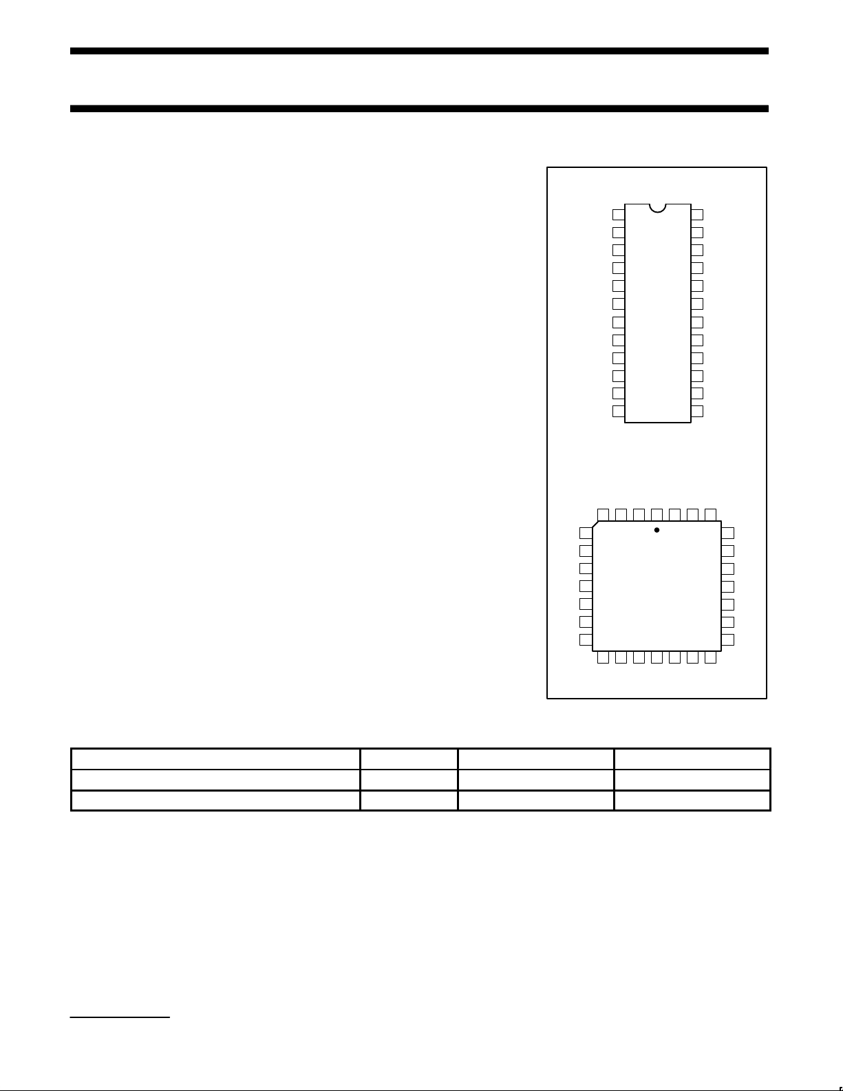
PIN CONFIGURATIONS
1234
5
6
7
8
9
10
11
12 13 14 15 16 17
18
19
20
21
22
23
24
25
262728
1
2
3
4
5
6
7
8
9
10
11
12 13
14
15
16
17
18
19
20
21
22
23
24
N Package
I0
I1
I2
I3
I4
I5
I6
I7
I8
I9
I10
V
CC
B9
B8
B7
B6
B5
B4
B3
B2
B1
B0
I11
GND
A Package
N = Plastic Dual In-Line (300mil-wide)
I0I1I2I3
V
CC
B9 B8
NC
I4
I5
I6
I7
I8
NC
I9 I10
GND
I11 B0 B1 B2
NC
B3
B7
B6
B5
B4
NC
A = Plastic Leaded Chip Carrier
ORDERING INFORMATION
DESCRIPTION tPD (MAX) ORDER CODE DRAWING NUMBER
24-Pin Plastic Dual In-Line 300mil-wide 10ns PLUS173–10N 0410D
28-Pin Plastic Leaded Chip Carrier 10ns PLUS173–10A 0401F
PAL is a registered trademark of Advanced Micro Devices Corporation.

Philips Semiconductors Programmable Logic Devices Product specification
PLUS173–10
Programmable logic array
(22 × 42 × 10)
October 22, 1993
42
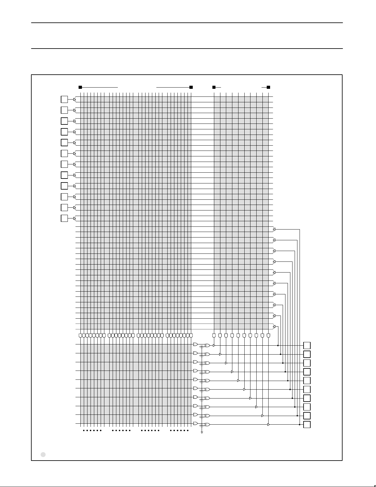
LOGIC DIAGRAM
NOTES:
1. All programmed ‘AND’ gate locations are pulled to logic “1”.
2. All programmed ‘OR’ gate locations are pulled to logic “0”.
3. Programmable connection.
(LOGIC TERMS–P) (CONTROL TERMS)
1
2
3
4
5
6
7
8
9
10
11
13
14
15
16
17
18
19
20
21
22
23
I0
I1
I2
I3
I4
I5
I6
I7
I8
I9
I10
I11
B9
B8
B7
B6
B5
B4
B3
B2
B1
B0
31 24 23 16 15 8 7 0
D9 D8 D7 D6 D5 D4 D3 D2 D1 D0
S9
S8
S7
S6
S5
S4
S3
S2
S1
S0
X9
X8
X7
X6
X5
X4
X3
X2
X1
X0
B9
B8
B7
B6
B5
B4
B3
B2
B1
B0

Philips Semiconductors Programmable Logic Devices Product specification
PLUS173–10
Programmable logic array
(22 × 42 × 10)
October 22, 1993
43
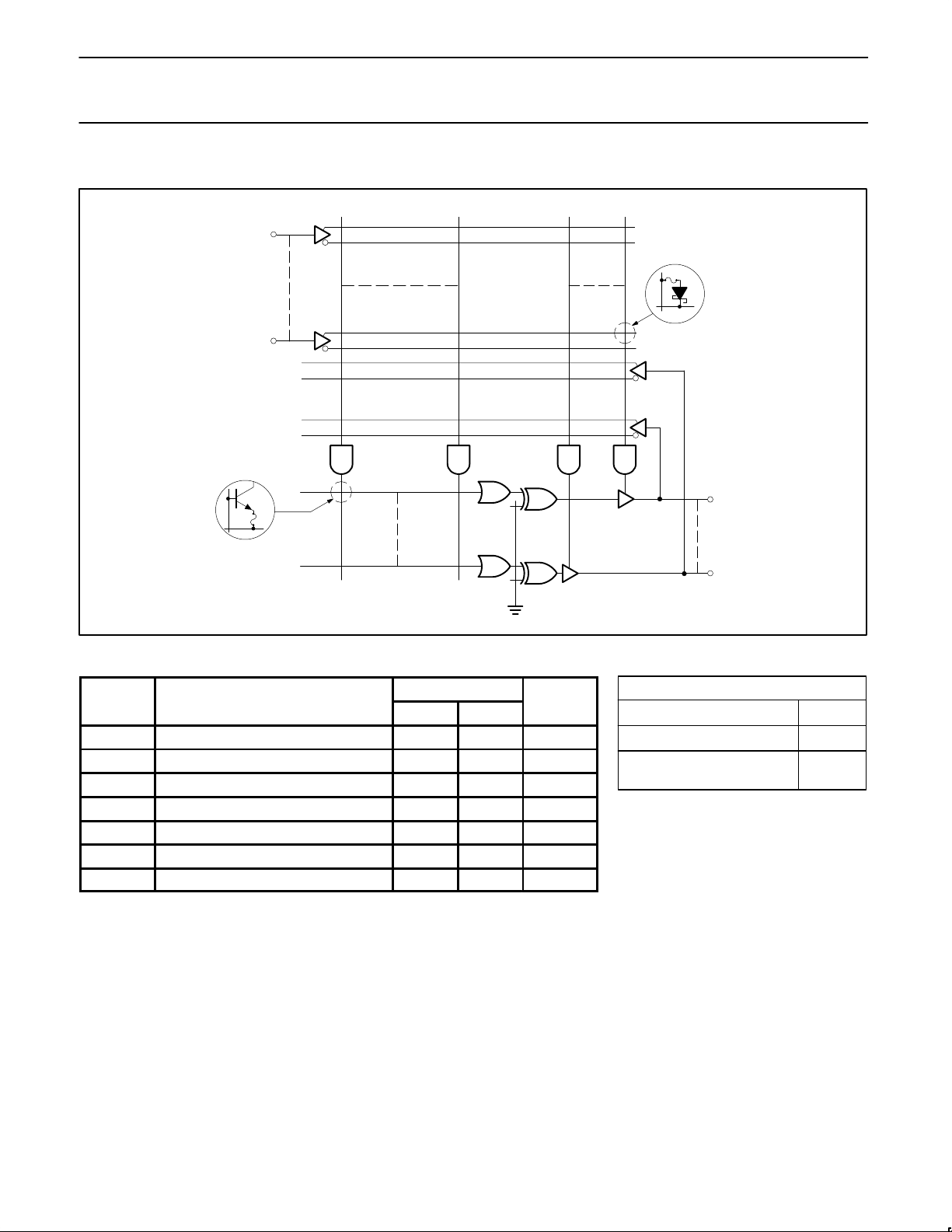
FUNCTIONAL DIAGRAM
P31 P0 D0 D9
I0
I11
B0
B9
B9
B0
S0
S9
X9
X0
ABSOLUTE MAXIMUM RATINGS
1
THERMAL RATINGS
RATING
SYMBOL PARAMETER Min Max UNIT
V
CC
Supply voltage +7 V
DC
V
IN
Input voltage +5.5 V
DC
V
OUT
Output voltage +5.5 V
DC
I
IN
Input currents –30 +30 mA
I
OUT
Output currents +100.0 mA
T
amb
Operating free-air temperature range 0 +75 °C
T
stg
Storage temperature range –65 +150 °C
NOTES:
1. Stresses above those listed may cause malfunction or permanent damage to the device. This
is a stress rating only. Functional operation at these or any other condition above those
indicated in the operational and programming specification of the device is not implied.
TEMPERATURE
Maximum junction 150°C
Maximum ambient 75
°C
Allowable thermal rise 75
°C
ambient to junction
 Loading...