

Philips PTN3500DH Datasheet

INTEGRATED CIRCUITS
PTN3500
Maintenance and control device
Product specification
Supersedes data of 2000 Nov 22
2001 Jan 17
Philips Semiconductors Product specification
Type number
PTN3500Maintenance and control device
FEA TURES
2
•I
C to parallel port expander
•Internal 256x8 E
2
PROM
•Self timed write cycle (5 ms typ.)
•Four byte page write operation
•Controlled pull-up on address lines
•Low voltage V
range of +2.5 V to +3.6 V
CC
•5 V – tolerant I/Os
•Low standby current (< 60 µA )
•Power on Reset
•Supports Live Insertion
•Compatible with SMBus specification version 1.1
•High E
2
PROM endurance and data retention
•Available in SO16 and TSSOP16 package options
DESCRIPTION
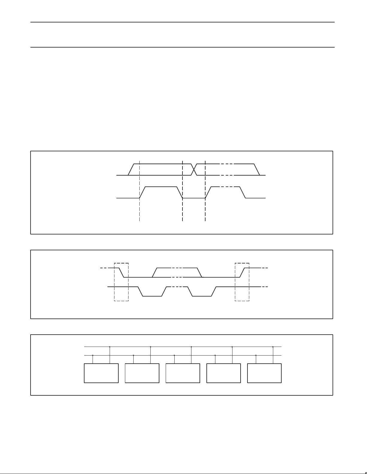
The PTN3500 is a general purpose maintenance and control device.
It features an on-board E
codes or board manufacturing data for read–back by application
software for diagnostic purposes.
The eight quasi bidirectional data pins can be independently
assigned as inputs or outputs to monitor board level status or
activate indicator devices such as LEDs.
The PTN3500 has three address pins allowing up to 8 devices to
share the common two wire I2C software protocol serial data bus.
The PTN3500 supports live insertion to facilitate usage in removable
cards on backplane systems.
2
PROM that can be used to store error
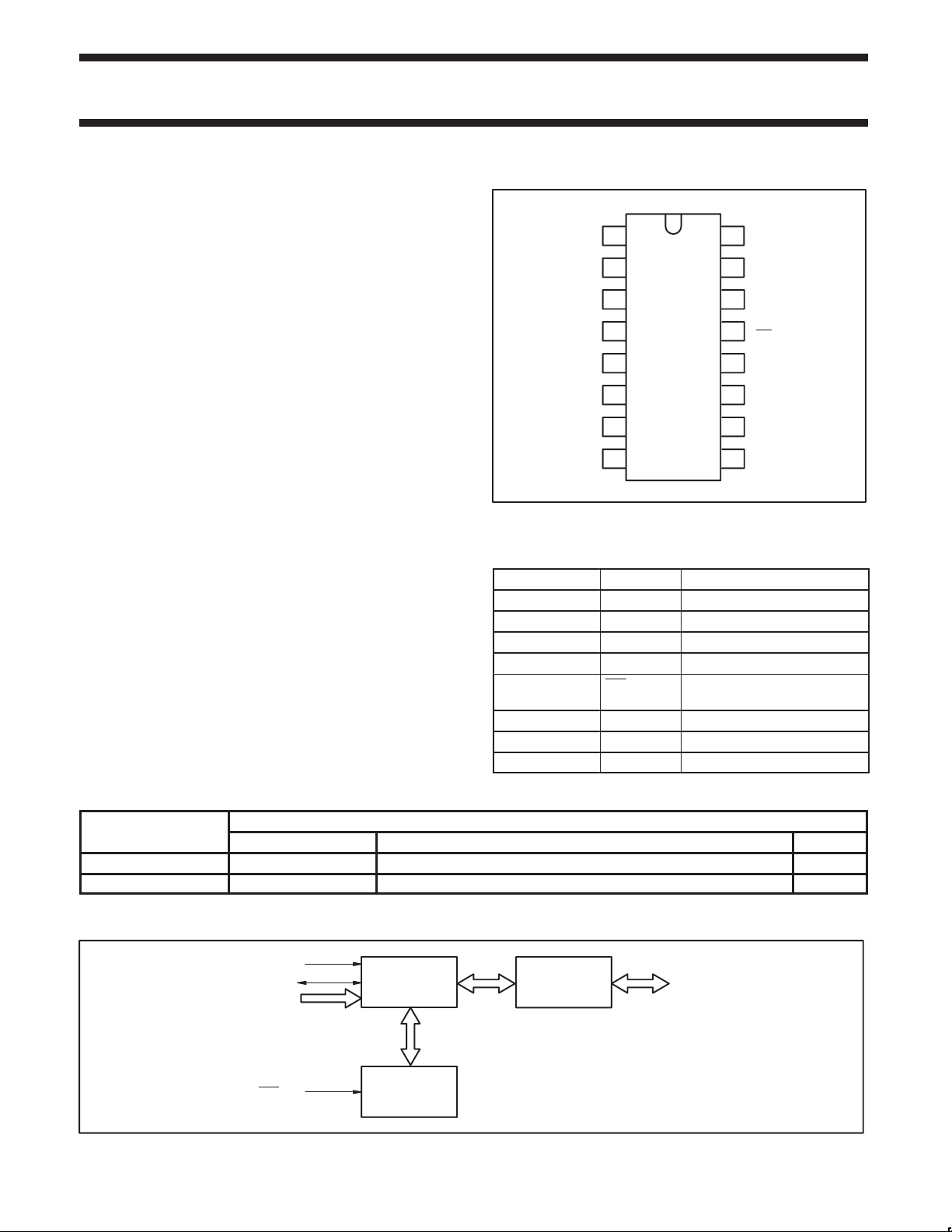
PIN CONFIGURATION
1
A0
2
A1
A2
3
4
P0
PTN3500
5
P1
P2
6
P3
7
V
SS
8
Figure 1.
V
16
DD
15
SDA
14
SCL
13
WC
12
P7
P6
11
10
P5
9
P4
SW00541
PIN DESCRIPTION
PIN NUMBER SYMBOL NAME AND FUNCTION
1,2,3 A0:2 Address Lines
4,5,6,7 P0:3 Quasi–bidirectional i/o pins
8 V
SS
9,10,1 1,12 P4:7 Quasi–bidirectional i/o pins
13 WC Write Control Pin. Should be
14 SCL I2C Serial Clock
15 SDA I2C Serial Data
16 V
DD
Supply Ground
tied LOW.
Supply Voltage
ORDERING INFORMATION
Package
Name Description Version
PTN3500D SO16 Plastic small-outline package; 16 leads; body width 7.5 mm SOT162-1
PTN3500DH TSSOP16 Plastic thin shrink small-outline package; 16 leads; body width 4.4 mm SOT403-1
FUNCTIONAL DIAGRAM
SCL
SDA
A2:0
WC
2
I
C
Control
E2PROM
256 x 8
Figure 2.
2001 Jan 17 853-2226 25435
2
8-Bit
I/O
Port
P7:0
SW00562
Philips Semiconductors Product specification
PTN3500Maintenance and control device
CHARACTERISTICS OF THE I2C-BUS
The I2C-bus is for 2-way, 2-line communication between different ICs
or modules. The two lines are a serial data line (SDA) and a serial
clock line (SCL). Both lines must be connected to a positive supply
via a pull-up resistor when connected to the output stages of a device.
Data transfer may be initiated only when the bus is not busy.
Bit transfer
One data bit is transferred during each clock phase. The data on the
SDA line must remain stable during the HIGH period of the clock
pulse as changes in the data line at this time will be interpreted as
control signals (See Figure 3).
SDA
Start and stop conditions
Both data and clock lines remain HIGH when the bus is not busy. A
HIGH-to-LOW transition of the data line, while the clock is HIGH is
defined as the start condition (S). A LOW-to-HIGH transition of the
data line while the clock is HIGH is defined as the stop condition (P)
(see Figure 4).
System configuration
A device generating a message is a “transmitter”, a device receiving
is the “receiver”. The device that controls the message is the
“master” and the devices which are controlled by the master are the
“slaves” (see Figure 5).
SDA
SCL
SDA
SCL
SCL
DATA LINE
STABLE;
DATA VALID
CHANGE
OF DATA
ALLOWED
Figure 3. Bit transfer
S
START CONDITION STOP CONDITION
P
Figure 4. Definition of start and stop conditions
SW00542
SDA
SCL
SW00543
2001 Jan 17
MASTER
TRANSMITTER/
RECEIVER
SLAVE
RECEIVER
SLAVE
TRANSMITTER/
RECEIVER
Figure 5. System configuration
3
MASTER
TRANSMITTER
MASTER
TRANSMITTER/
RECEIVER
SW00544
Philips Semiconductors Product specification
PTN3500Maintenance and control device
Acknowledge (see Figure 6)
The number of data bytes transferred between the start and the stop
conditions from transmitter to receiver is not limited. Each byte of
eight bits is followed by one acknowledge bit. The acknowledge bit
is a HIGH level put on the bus by the transmitter whereas the
master generates an extra acknowledge related clock pulse.
A slave receiver which is addressed must generate an acknowledge
after the reception of each byte. Also a master must generate an
acknowledge after the reception of each byte that has been clocked
DATA OUTPUT
BY TRANSMITTER
DATA OUTPUT
BY RECEIVER
SCL FROM
MASTER
S
START
CONDITION
Figure 6. Acknowledgment on the I2C-bus
out of the slave transmitter. The device that acknowledges has to
pull down the SDA line during the acknowledge clock pulse, so that
the SDA line is stable LOW during the HIGH period of the
acknowledge related clock pulse, set–up and hold times must be
taken into account.
A master receiver must signal an end of data to the transmitter by
not generating an acknowledge on the last byte that has been
clocked out of the slave. In this event the transmitter must leave the
data line HIGH to enable the master to generate a stop condition.
NOT ACKNOWLEDGE
ACKNOWLEDGE
9821
CLOCK PULSE FOR
ACKNOWLEDGEMENT
SW00545
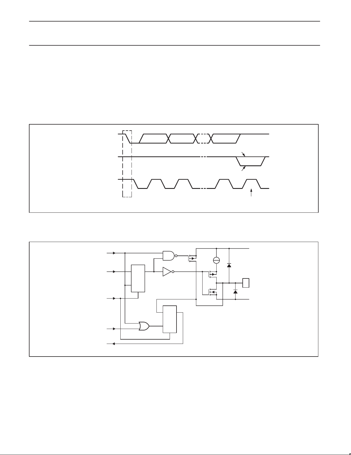
FUNCTIONAL DESCRIPTION
WRITE PULSE
DATA FROM
SHIFT REGISTER
POWER-ON
RESET
READ PULSE
DATA TO
SHIFT REGISTER
100 µA
DQ
FF
C
I
S
DQ
FF
C
I
S
Figure 7. Simplified schematic diagram of each I/O
V
DD
P0 TO P7
V
SS
SW00546
2001 Jan 17
4
Philips Semiconductors Product specification
PTN3500Maintenance and control device
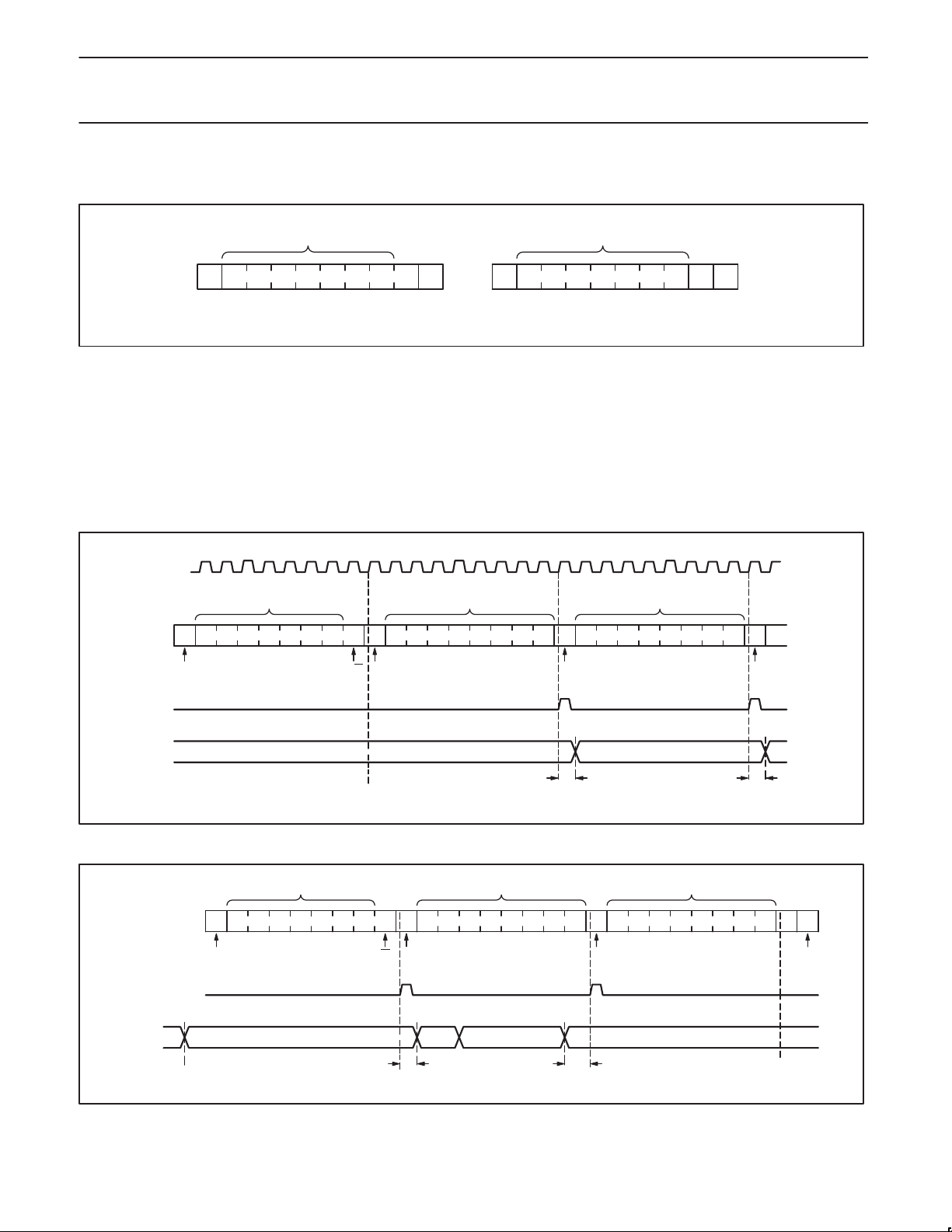
Addressing
For addressing, see Figure 8.
SLAVE ADDRESSSLAVE ADDRESS
S 0 1 0 0 A2 A1 A0 0 A 0 0 AS 1 1 0 A2 A1 A0
(a) I/O EXPANDER
(b) MEMORY
a. b.
SW00547
Figure 8. PTN3500 slave addresses
Asynchronous Start
Following any Start condition on the bus, a minimum of 9 SCL clock cycles must be completed before a Stop condition can be issued. The
device does not support a Stop or a repeated Start condition during this time period.
I/O OPERATIONS (see also Figure 7)
Each of the PTN3500’s eight I/Os can be independently used as an input or output. Input I/O data is transferred from the port to the
microcontroller by the READ mode (See Figure 10). Output data is transmitted to the port by the I/O WRITE mode (see Figure 9).
WRITE TO
PORT
DATA OUT
FROM PORT
SCL
12345678
SLAVE ADDRESS (I/O EXPANDER)
S 0 1 0 0 A2 A1 A0 0 A DATA 1 A DAT A 2 ASDA
DATA TO PORT
ACKNOWLEDGE
R/WSTART CONDITION ACKNOWLEDGE
FROM SLAVE
t
pv
FROM SLAVE
DATA TO PORT
t
pv
ACKNOWLEDGE
FROM SLAVE
DATA 2 VALIDDATA 1 VALID
READ FROM
PORT
DATA INTO
PORT
2001 Jan 17
Figure 9. I/O WRITE mode (output)
SLAVE ADDRESS (I/O EXPANDER) DATA FROM PORT DATA FROM PORT
S 0 1 0 0 A2 A1 A0 1 A DATA 1 A
START CONDITION ACKNOWLEDGE
DATA 1
R/W ACKNOWLEDGE
t
ph
FROM SLAVE
DATA 2 DATA 3
FROM MASTER
t
ps
Figure 10. I/O READ mode (input)
5
DATA 4
DATA 4
SW00548
1SDA
P
STOP
CONDITION
SW00549
 Loading...