Philips PTN3310D, PTN3311D Datasheet

INTEGRATED CIRCUITS
PTN3310/PTN3311
High-speed serial logic translators
Product data
2001 Jun 19

Philips Semiconductors Product data
Type number
PTN3310/PTN331 1High-speed serial logic translators
FEA TURES
•Meets LVDS EIA-644 and PECL standards
•2 pin-for-pin replacement input/output choices:
– LVDS in, PECL out (PTN3310)
– PECL in, LVDS out (PTN3311)
•Single +3.3 V supply voltage operation
•Available in 8-pin SO package
•Maximum throughput data rate of 800 Mbps typical
APPLICATIONS
•High-speed networking and telecom applications
– ATM
– SONET/SDH
– Switches
– Routers
– Add-drop multiplexers
GENERAL DESCRIPTION
The High-Speed Serial Logic Translator provides a point solution
that addresses the various interface logic requirements of Optical
Transceiver Modules. The product offers a compact translation
between LVDS and PECL high speed serial data lines. This provides
the end users a simple way to mix or match Optical Transceiver ICs
from various vendors to maximize desired performance and reduces
the need to redesign interfaces to accommodate new Optical
Transceiver ICs.
The High-Speed Serial Logic Translator comes in two translation
choices to allow mixing LVDS and PECL input/outputs. The product
is offered in a small, convenient, 8-pin package.
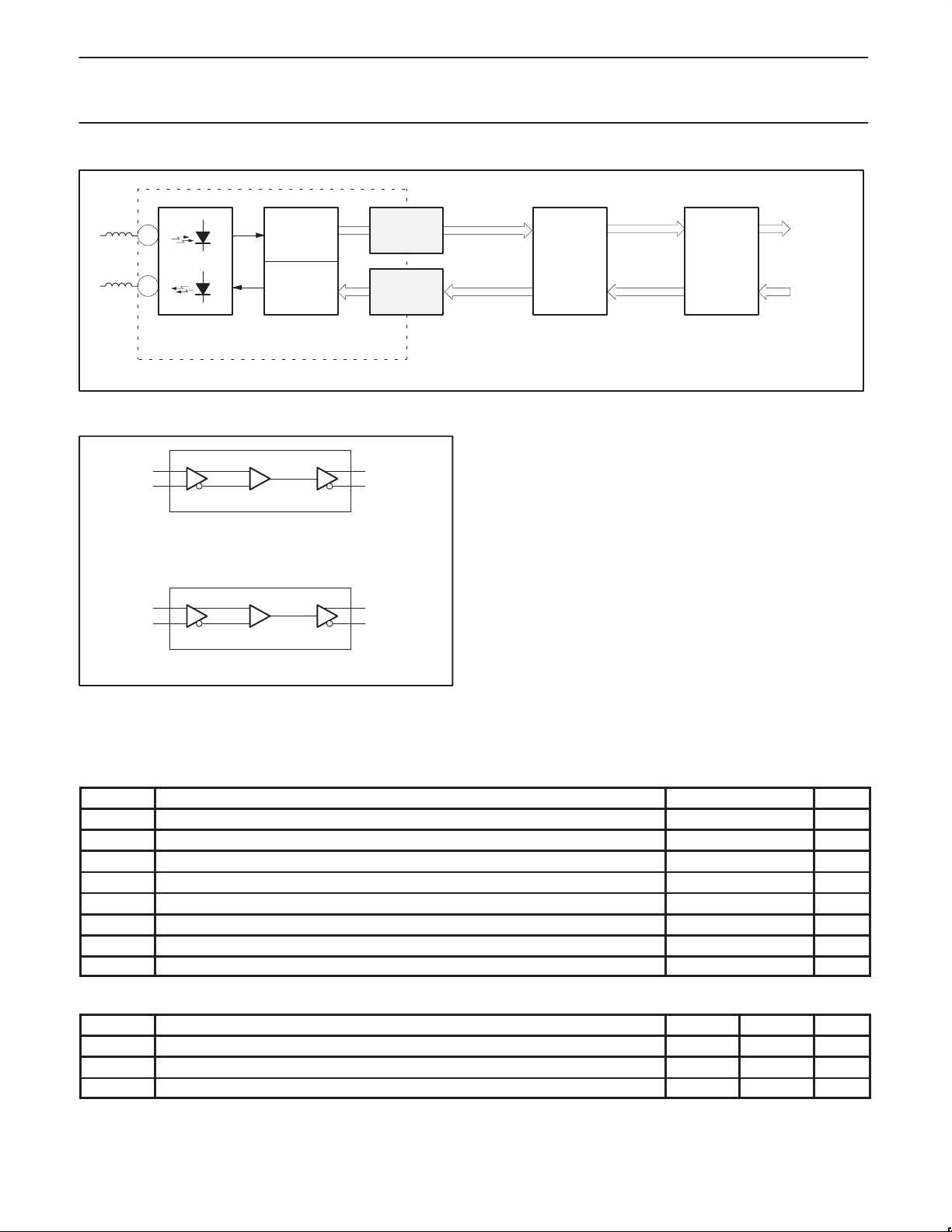
Figure 1 shows the High-Speed Serial Logic Translator Device in a
typical high speed optical module application. Figure 2 shows the
circuit block diagrams.
PIN CONFIGURATIONS
1
GND1
2
V
INP
3
V
INN
4
GND2
1
GND1
2
V
INP
3
V
INN
4
GND2
8-pin SO package
PTN3310
PTN3311
8
7
6
5
8
7
6
5
ST00014
V
V
V
V
V
V
V
V
CC1
OUTP
OUTN
CC2
CC1
OUTP
OUTN
CC2
PIN DESCRIPTIONS
8-pin SO package
Pin # Symbol Name and function
1, 4 GND1, GND2 Ground
2, 3 V
5, 8 V
6, 7 V
, V
INP
CC1
OUTN
, V
INN
, V
CC2
OUTP
Differential inputs
Supply voltage
Differential outputs
ORDERING INFORMATION
Package
Name Description Version
PTN3310D SO8 Plastic small-outline package; 8 leads; body width 3.9 mm SOT96-1
PTN3311D SO8 Plastic small-outline package; 8 leads; body width 3.9 mm SOT96-1
2001 Jun 19 853-2264 26562
2

Philips Semiconductors Product data
PTN3310/PTN3311High-speed serial logic translators
Optical
RCVR
Translator
Optical
Laser
Driver
Translator
Optical Interface IC’s
1 x 9 Optical Module
Figure 1. High-Speed Serial Logic Translators in Optical Module Application
LVDS IN PECL OUT
PTN3310
PECL IN LVDS OUT
PTN3311
ST00009
Figure 2. High-Speed Serial Logic Translator Block Diagrams
MAC
(ASIC)
Serial
Backplane
Device
ST00040
To/From
Serial
Backplane
ABSOLUTE MAXIMUM RATINGS
Symbol Parameter Limits Unit
V
CC
V
I
V
O
t
SC
T
j
T
stg
ESD
ESD
HBM
MM
Supply voltage –0.3 to +4.0 V
LVDS receiver input voltage –0.3 to +5.5 V
LVDS driver output voltage –0.3 to +5.5 V
LVDS output short circuit duration continuous
Maximum junction temperature +150 °C
Storage temperature range –65 to +150 °C
Electrostatic discharge (Human Body Model, 1.5 kΩ, 100 pF) >2 kV
Electrostatic discharge (Machine Model, 0 kΩ, 200 pF) >200 V
RECOMMENDED OPERATING CONDITIONS
Symbol Parameter Min Max Unit
V
CC
T
amb
V
CCN
2001 Jun 19
Supply voltage 3.0 3.6 V
Operating ambient temperature range in free air –40 +85 °C
Power supply noise voltage – 100 mV
3
PP
 Loading...