

Philips PTN2111BD Datasheet
INTEGRATED CIRCUITS
PTN2111
1:10 LVDS clock distribution device
Product Data
2001 Jun 19
Philips Semiconductors Product Data
PTN21 111:10 LVDS clock distribution device
FEA TURES
•100 ps part-to-part skew
•35 ps output-to-output skew
•Differential design
•Meets LVDS specification for driver outputs and receiver inputs
•Reference voltage available output V
•Low voltage V
range of +2.375 V to 2.625 V
CC
BB
•High signalling rate capability (above 622 MHz)
•Supports open, short, and terminated input fail-safe (HIGH output
state)
•Programmable drivers power off control
•Available in LQFP32 package
DESCRIPTION
The PTN2111 is a low skew programmable 1:10 LVDS clock
distribution device. The selected input signal is fanned out to 10
identical differential outputs.
The PTN2111 features an 11-bit Shift Register with a serial-in and a
Control Register. The purpose of the Control Register is to enable or
power off each output clock channel and to select the clock input.
The PTN2111 is specifically designed, modeled and produced with
low skew as the key goal. Optimal design and layout serve to
minimize gate-to-gate skew within a device. The final result is a
dependable guaranteed low skew device.
The PTN2111 can be used for high performance clock distribution in
+2.5 V systems with LVDS levels. Designers can take advantage of
the device’s performance to distribute low skew clocks across the
backplane or the board.
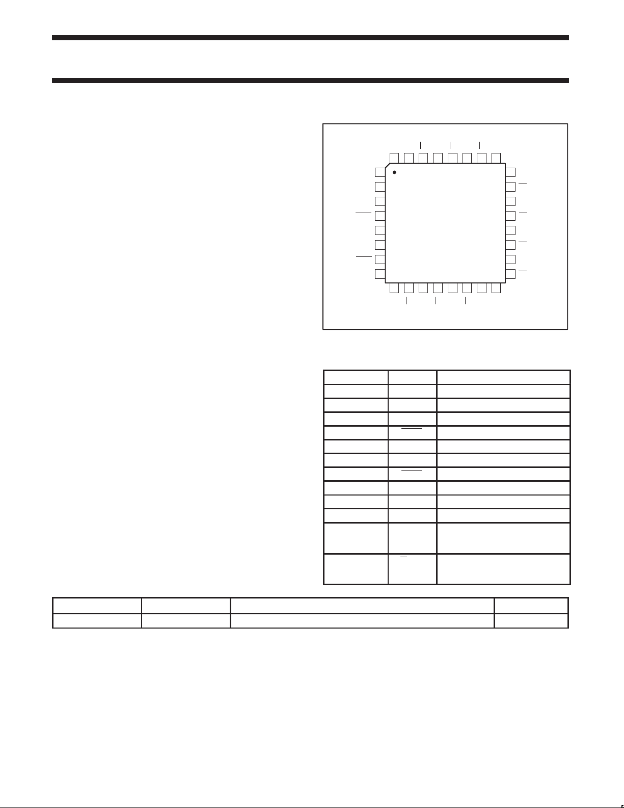
PIN CONFIGURATION
CC
Q0
Q0
Q1
Q1
Q2
Q2
27
14
Q7
26
15
Q7
GND
25
24
23
22
21
20
19
18
17 Q6
16
CC
V
ST00013
Q3
Q3
Q4
Q4
Q5
Q5
Q6
CLK0
CLK0
V
CLK1
CLK1
CK
V
32
31
30
29
28
1
2
SI
3
4
5
BB
6
7
8EN
9
11
10
12
13
Q9
Q9
Q8
GND
Q8
PIN DESCRIPTION
PIN NUMBER SYMBOL NAME AND FUNCTION
1 CK Control register clock
2 SI Control register serial-in/CLK_SEL
3 CLK0 Differential input
4 CLK0 Differential input
5 V
6 CLK1 Differential input
7 CLK1 Differential input
8 EN Device enable/program
9, 25 GND Ground
16, 32 V
31, 29, 27, 24,
Q[0:9] Differential outputs
22, 20, 18, 15,
13, 11
30, 28, 26, 23,
Q[0:9] Differential outputs
21, 19, 17, 14,
12, 10
Output reference voltage
BB
Supply voltage
CC
TYPE NUMBER NAME DESCRIPTION VERSION
PTN2111BD LQFP32 Plastic low profile quad flat package; 32 leads; body 7 x 7 x 1.4 mm SOT358-1
2001 Jun 19 853-2263 26561
2
Philips Semiconductors Product Data
PTN21111:10 LVDS clock distribution device
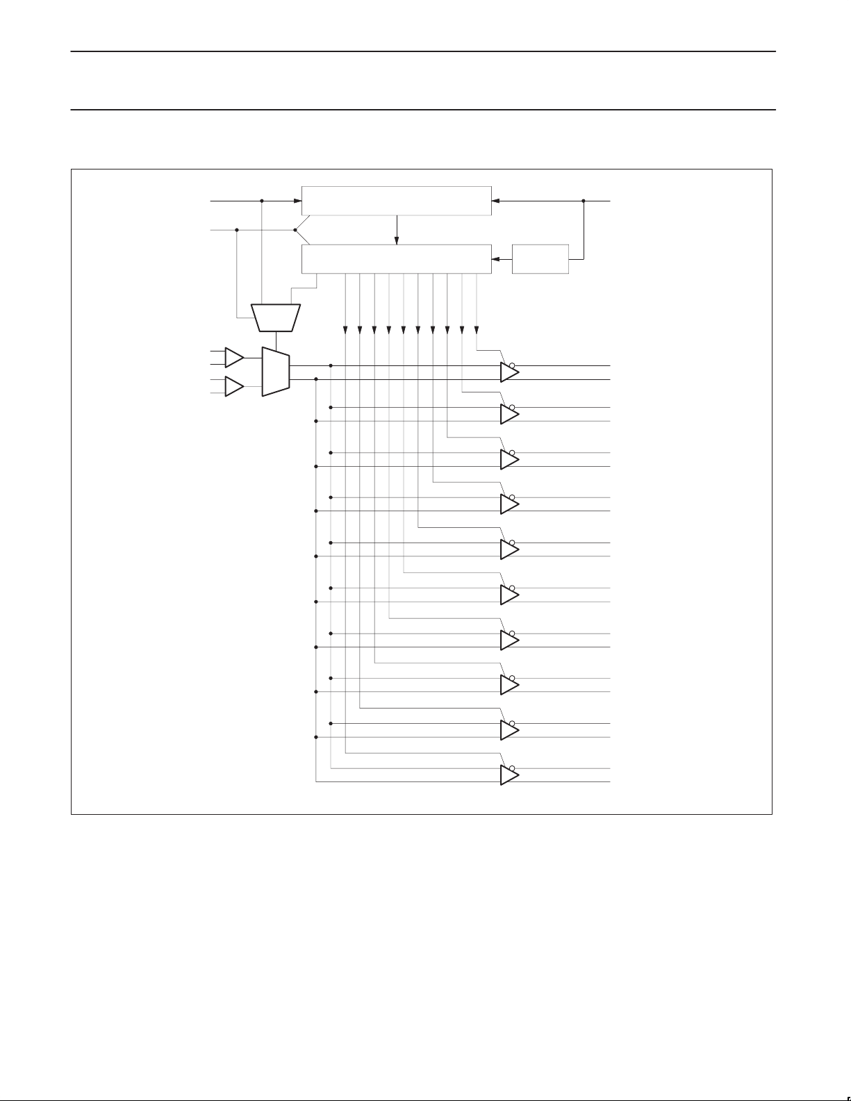
LOGIC DIAGRAM
EN
CLK0
CLK1
SI
01
SEL
0
1
Shift Register 11-Bit
Control Register 11-Bit
10
9876543210
CK
Counter
12
Q9
Q8
Q7
Q6
Q5
Q4
Q3
Q2
Q1
Q0
ST00010
2001 Jun 19
3
 Loading...