

Philips PTB32001X, PTB32003X, PTB32005X Datasheet

DISCRETE SEMICONDUCTORS
DATA SH EET
PTB32001X; PTB32003X;
PTB32005X
NPN microwave power transistors
Product specification
Supersedes data of November 1994
1997 Feb 18
Philips Semiconductors Product specification
NPN microwave power transistors
FEATURES
• Diffused emitter ballasting resistors providing excellent
current sharing and withstanding a high VSWR
• Interdigitated structure provides high emitter efficiency
• Multicell geometry gives good balance of dissipated
power and low thermal resistance
• Localized thick oxide auto-alignment process and gold
sandwich metallization ensure an optimum temperature
profile and excellent performance and reliability.
APPLICATIONS
Common-base, class B power amplifiers up to 4.2 GHz.
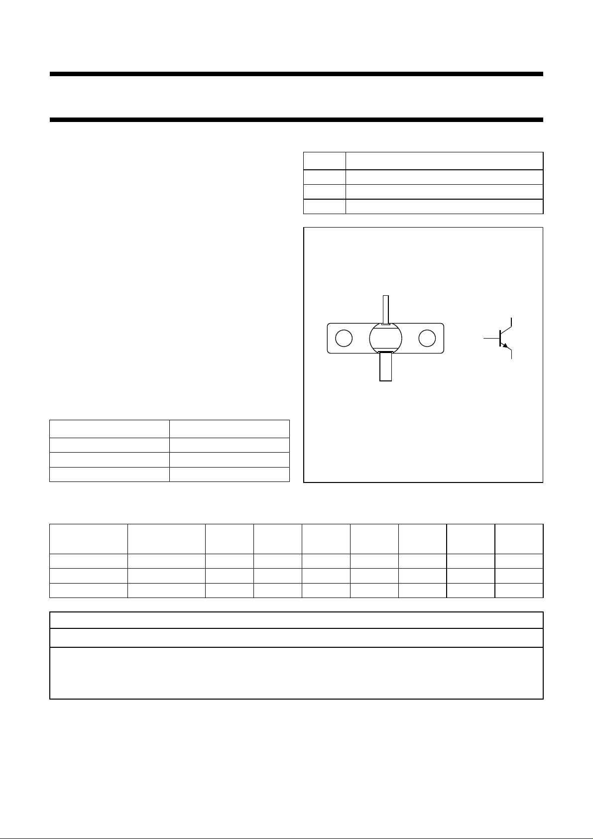
DESCRIPTION
NPN silicon planar epitaxial microwave power transistor in
a metal ceramic SOT440A flange package with base
connected to the flange.
PTB32001X; PTB32003X;
PINNING - SOT440A
PIN DESCRIPTION
1 collector
2 emitter
3 base connected to flange
lumns
Top view
1
3
2
PTB32005X
c
b
e
MAM131
MARKING
TYPE NUMBER MARKING CODE
PTB32001X 3201X
PTB32003X 3203X
Fig.1 Simplified outline and symbol.
PTB32005X 3205X
QUICK REFERENCE DATA
Microwave performance up to T
TYPE NUMBER
MODE OF
OPERATION
=25°C in a common-base class B circuit.
mb
f
(GHz)
V
(V)
CC
P
(W)
L
G
po
(dB)
η
(%)
C
Z
i
(Ω)
Z
(Ω)
PTB32001X CW 3 24 ≥1.3 ≥8 ≥35 15 + j31 5.5 + j10
PTB32003X CW 3 24 ≥2.5 ≥8 ≥35 5.5 + j29 5 − j2.2
PTB32005X CW 3 24 ≥4.5 ≥8 ≥35 2.8 + j20 4 − j7
WARNING
Product and environmental safety - toxic materials
This product contains beryllium oxide. The product is entirely safe provided that the BeO slab is not damaged.
All persons who handle, use or dispose of this product should be aware of its nature and of the necessary safety
precautions. After use, dispose of as chemical or special waste according to the regulations applying at the location of
the user. It must never be thrown out with the general or domestic waste.
L
1997 Feb 18 2
Philips Semiconductors Product specification
NPN microwave power transistors
PTB32001X; PTB32003X;
PTB32005X
LIMITING VALUES
In accordance with the Absolute Maximum Rating System (IEC 134).
SYMBOL PARAMETER CONDITIONS MIN. MAX. UNIT
V
V
V
V
I
P
T
T
T
CBO
CEO
CES
EBO
C
tot
stg
j
sld
collector-base voltage open emitter − 40 V
collector-emitter voltage open base − 15 V
collector-emitter voltage RBE=0Ω−40 V
emitter-base voltage open collector − 3.0 V
collector current (DC)
PTB32001X − 0.25 A
PTB32003X − 0.5 A
PTB32005X − 0.75 A
total power dissipation Tmb≤ 75 °C; f > 1 MHz
PTB32001X − 4.2 W
PTB32003X − 7.6 W
PTB32005X − 8.7 W
storage temperature range −65 +200 °C
operating junction temperature − 200 °C
soldering temperature t ≤ 10 s; note 1 − 235 °C
Note
1. Up to 0.3 mm from ceramic.
P
(W)
6
tot
4
2
0
−50
0 200
50 100 150
handbook, halfpage
MLC091
Tmb (
10
handbook, halfpage
P
tot
(W)
5
0
o
C)
50 200
0 50 100 150
MLC092
Tmb (
o
C)
f >1 MHz.
Fig.2 Power derating curve; PTB32001X.
1997 Feb 18 3
f > 1 MHz.
Fig.3 Power derating curve; PTB32003X.

Philips Semiconductors Product specification
NPN microwave power transistors
10
handbook, halfpage
P
tot
(W)
5
0
−50 200
0 50 100 150
MLC093
Tmb (
o
C)
PTB32001X; PTB32003X;
PTB32005X
f > 1 MHz.
Fig.4 Power derating curve; PTB32005X.
THERMAL CHARACTERISTICS
SYMBOL PARAMETER CONDITIONS MAX. UNIT
R
th j-mb
thermal resistance from junction to mounting base Tj=75°C
PTB32001X 22 K/W
PTB32003X 12 K/W
PTB32005X 10.5 K/W
R
th mb-h
thermal resistance from mounting base to heatsink Tj=75°C; note 1 0.7 K/W
Note
1. See
“Mounting recommendations in the General part of handbook SC19a”
.
1997 Feb 18 4
 Loading...