

Philips PTB23006U Datasheet

DISCRETE SEMICONDUCTORS
DATA SH EET
PTB23006U
Microwave power transistor
Preliminary specification
Supersedes data of December 1994
1997 Feb 19
Philips Semiconductors Preliminary specification
Microwave power transistor PTB23006U
FEATURES
• Very high power gain
• Diffused emitter ballasting resistors
improve ruggedness
• Interdigitated emitter-base
structure
• Gold metallization with barrier layer
to prevent electromigration and
gold diffusion during life
• Multicell geometry improves power
sharing and reduces thermal
resistance
• Internal input prematching network.
APPLICA TIONS
Intended for use in common-base,
class C power amplifiers at
frequencies up to 2.3 GHz.
DESCRIPTION
NPN silicon planar epitaxial
microwave power transistor in a
SOT440A hermetically sealed metal
ceramic flange package, with base
connected to flange.
QUICK REFERENCE DATA
Microwave performance up to T
=25°C in a common-base class C
mb
narrowband amplifier.
MODE OF
OPERATION
f
(GHz)
V
(V)
CC
P
(W)
L
G
(dB)
p
η
C
(%)
Zi; Z
(Ω)
Class C (CW) 2 28 >5 >9 >40 see Figs 5
and 6
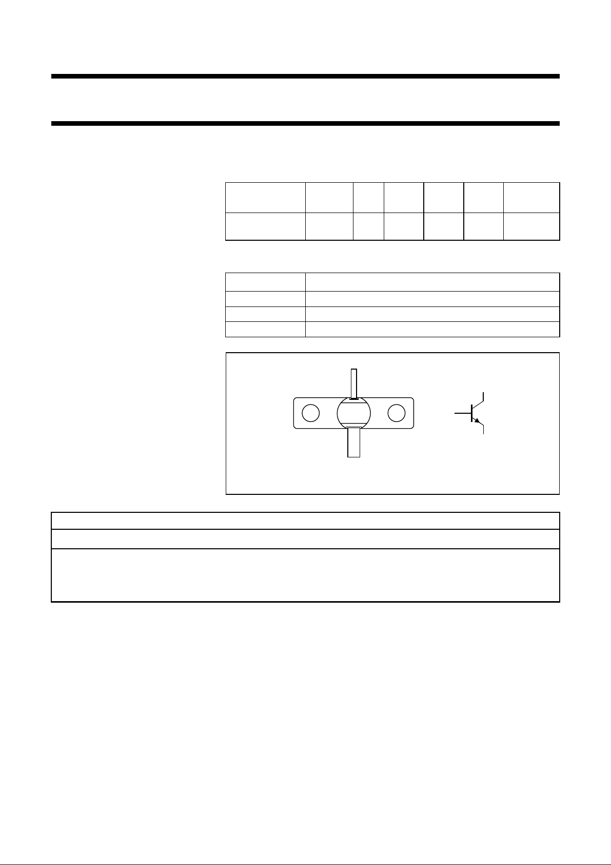
PINNING - SOT440A
PIN DESCRIPTION
1 collector
2 emitter
3 base connected to flange
handbook, 4 columns
Top view
1
c
b
3
2
MAM131
e
Fig.1 Simplified outline and symbol.
L
WARNING
Product and environmental safety - toxic materials
This product contains beryllium oxide. The product is entirely safe provided that the BeO disc is not damaged.
All persons who handle, use or dispose of this product should be aware of its nature and of the necessary safety
precautions. After use, dispose of as chemical or special waste according to the regulations applying at the location of
the user. It must never be thrown out with the general or domestic waste.
1997 Feb 19 2
Philips Semiconductors Preliminary specification
Microwave power transistor PTB23006U
LIMITING VALUES
In accordance with the Absolute Maximum Rating System (IEC 134).
SYMBOL PARAMETER CONDITIONS MIN. MAX. UNIT
V
CBO
V
CES
V
CEO
V
EBO
I
C
P
tot
T
stg
T
j
T
sld
Note
1. Up to 0.2 mm from ceramic.
collector-base voltage open emitter − 40 V
collector-emitter voltage RBE=0 − 40 V
collector-emitter voltage open base − 15 V
emitter-base voltage open collector − 3V
collector current − 0.75 A
total power dissipation Tmb=75°C − 11 W
storage temperature −65 +200 °C
junction temperature − 200 °C
soldering temperature t ≤ 10 s; note 1 − 235 °C
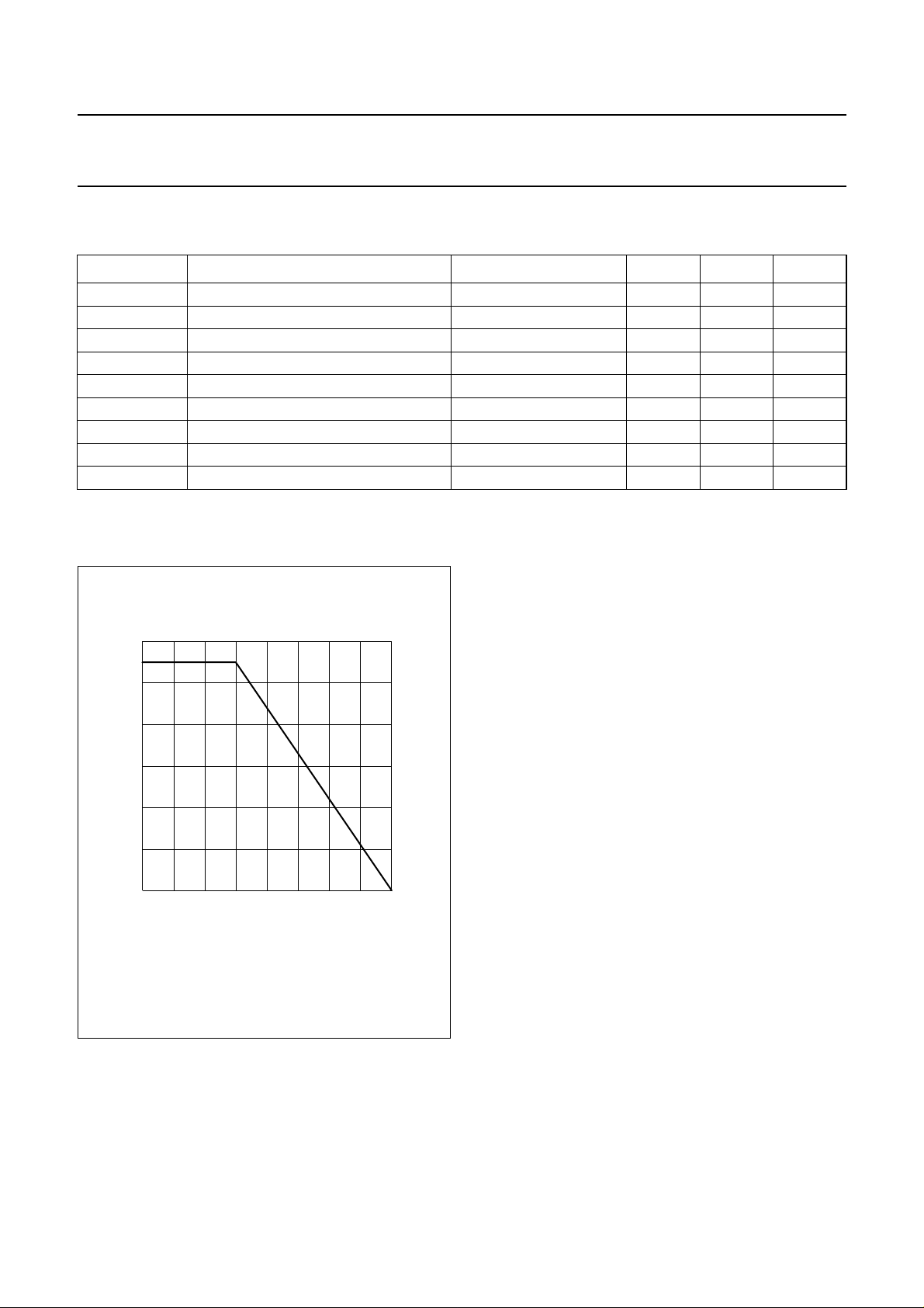
12
handbook, halfpage
P
tot
(W)
8
4
0
0 50 100 200
150
T ( C)
Fig.2 Power derating curve.
mb
MLC461
o
1997 Feb 19 3

Philips Semiconductors Preliminary specification
Microwave power transistor PTB23006U
THERMAL CHARACTERISTICS
SYMBOL PARAMETER CONDITIONS MAX. UNIT
R
th j-mb
R
th mb-h
Note
1. See
“Mounting recommendations in the General part of handbook SC19a”.
CHARACTERISTICS
=25°C unless otherwise specified.
T
mb
SYMBOL PARAMETER CONDITIONS MIN. MAX. UNIT
I
CES
V
(BR)CBO
V
(BR)CES
V
(BR)EBO
h
FE
thermal resistance from junction to mounting base Tj=75°C 8.5 K/W
thermal resistance from mounting base to heatsink note 1 0.7 K/W
collector cut-off current IE= 0; VCE=30V − 300 µA
collector-base breakdown voltage IC= 3 mA; IE=0 40 − V
collector-emitter breakdown voltage IC= 3 mA; RBE=0 40 − V
emitter-base breakdown voltage IC= 1.5 mA 3 − V
DC current gain IC= 450 mA; VCE= 3 V 15 150
APPLICATION INFORMATION
Microwave performance up to T
MODE OF
OPERATION
f
(GHz)
=25°C in a common-base class C test circuit.
mb
V
CE
(V)
class C (CW) 2 28 >5
typ. 5.8
P
(W)
L
G
p
(dB)
>9
typ. 10.5
η
C
(%)
>40
typ. 45
Zi; Z
L
(Ω)
see Figs 5
and 6
1997 Feb 19 4
 Loading...