

Philips PPC5001T Datasheet
DISCRETE SEMICONDUCTORS
DATA SH EET
PPC5001T
NPN microwave power transistor
Product specification
Supersedes data of November 1994
File under Discrete Semiconductors, SC15
1997 Mar 03
Philips Semiconductors Product specification
NPN microwave power transistor PPC5001T
FEATURES
• Diffused emitter ballasting resistors providing excellent
current sharing and withstanding a high VSWR
• Interdigitated structure provides high emitter efficiency
• Gold metallization realizes very stable characteristics
and excellent lifetime
• Multicell geometry gives good balance of dissipated
power and low thermal resistance
APPLICATIONS
Intended for use in common-collector oscillator circuits in
military and professional applications up to 5 GHz.
DESCRIPTION
NPN silicon planar epitaxial microwave power transistor in
a SOT447A metal ceramic flange package.
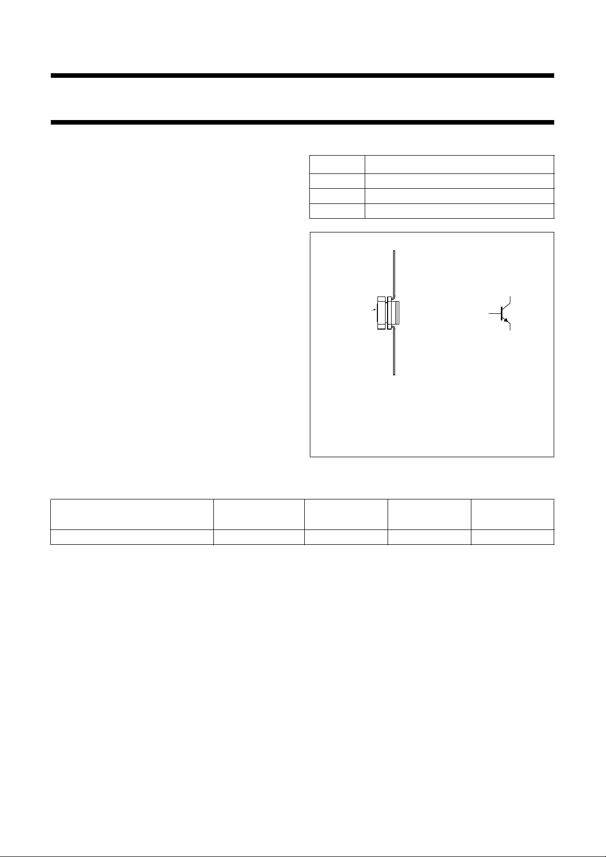
PINNING - SOT447A
PIN DESCRIPTION
1 base
2 emitter
3 collector
handbook, halfpage
Marking code: 395
3
1
2
Side view
c
b
e
MAM331
Fig.1 Simplified outline and symbol.
QUICK REFERENCE DATA
Microwave performance up to T
MODE OF OPERATION
=25°C in an oscillator circuit up to 5 GHz; typical values.
mb
f
(GHz)
V
(V)
CE
I
C
(mA)
(mW)
Class A (CW) 5 20 200 450
P
L
1997 Mar 03 2
Philips Semiconductors Product specification
NPN microwave power transistor PPC5001T
LIMITING VALUES
In accordance with the Absolute Maximum Rating System (IEC 134).
SYMBOL PARAMETER CONDITIONS MIN. MAX. UNIT
V
CBO
V
CER
V
CEO
V
EBO
I
C
P
tot
T
stg
T
j
T
sld
Note
1. At 0.1 mm from the case.
collector-base voltage open emitter − 40 V
collector-emitter voltage RBE=70Ω−35 V
collector-emitter voltage open emitter − 16 V
emitter-base voltage open collector − 3V
collector current (DC) − 0.25 A
total power dissipation T
≤ 75 °C − 4W
amb
storage temperature −65 +200 °C
junction temperature − 200 °C
soldering temperature t ≤ 10 s; note 1 − 235 °C
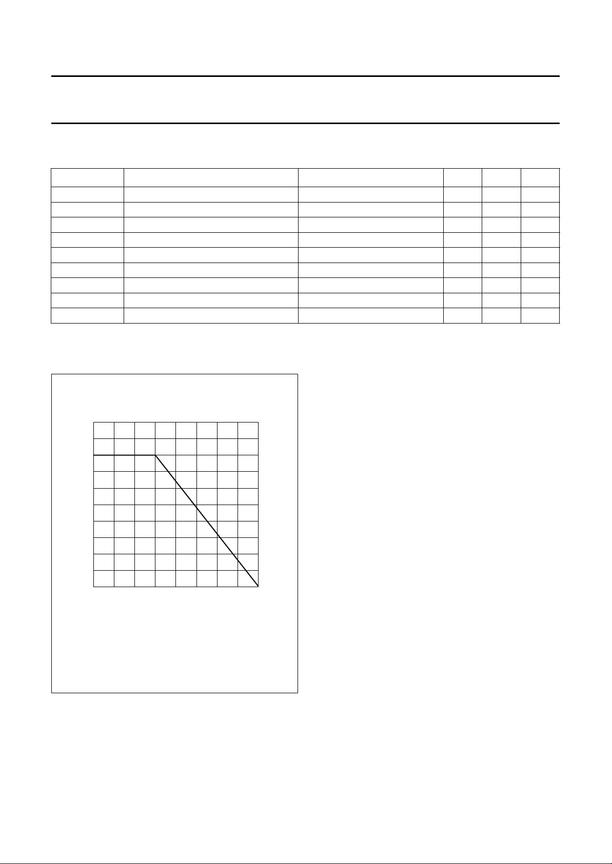
handbook,
5
P
tot max
(W)
4
3
2
1
0
0 50 100 200
150
Tmb (°C)
Fig.2 Power dissipation derating as a function of
mounting-base temperature.
MGD975
1997 Mar 03 3
 Loading...