

Philips PMEM4010PD Technical data
查询PMEM4010PD供应商
DISCRETE SEMICONDUCTORS
DATA SH EET
ook, halfpage
M3D302
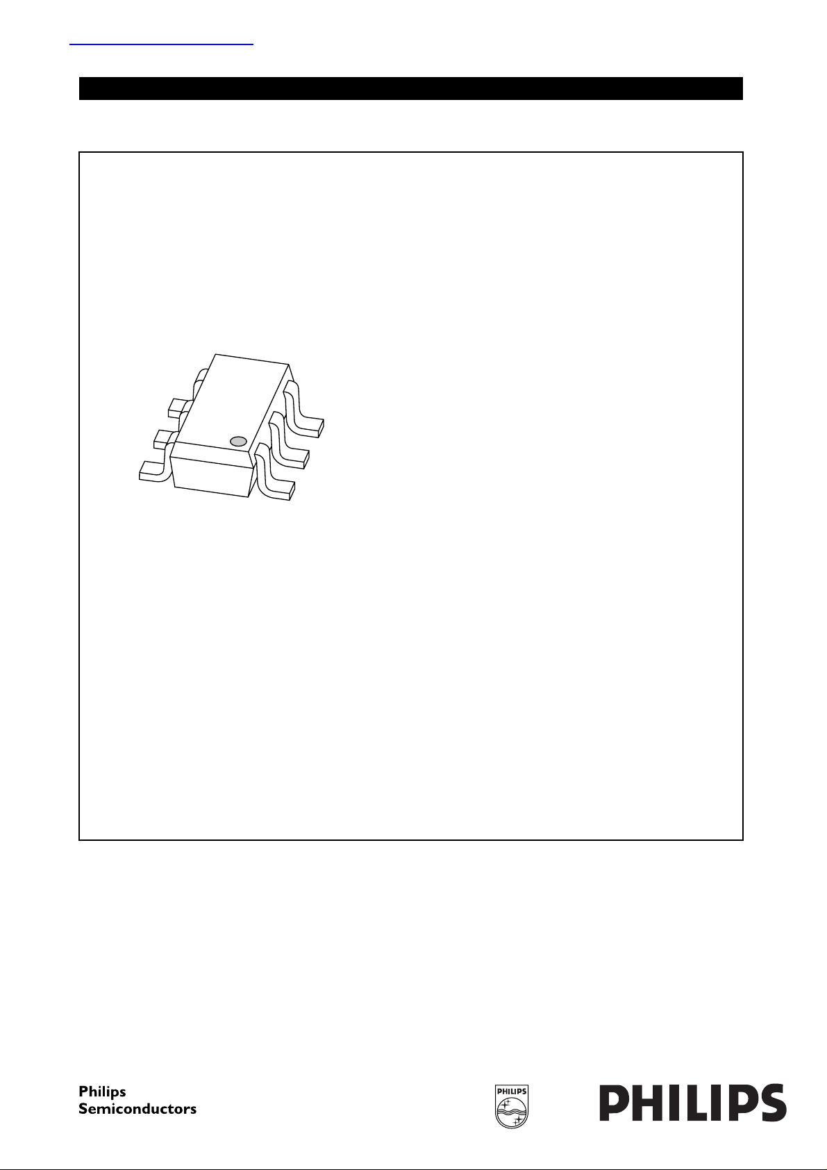
PMEM4010PD
PNP transistor/Schottky diode
module
Product specification 2002 Oct 28
Philips Semiconductors Product specification
PNP transistor/Schottky diode module PMEM4010PD
FEATURES
• 600 mW total power dissipation
• High current capability
• Reduces required PCB area
• Reduced pick and place costs
• Small plastic SMD package.
Transistor:
• Low collector-emitter saturation voltage.
Diode:
• Ultra high-speed switching
• Very low forward voltage
• Guard ring protected.
APPLICATIONS
• DC/DC convertors
• Inductive load drivers
• General purpose load drivers
• Reverse polarity protection circuits.
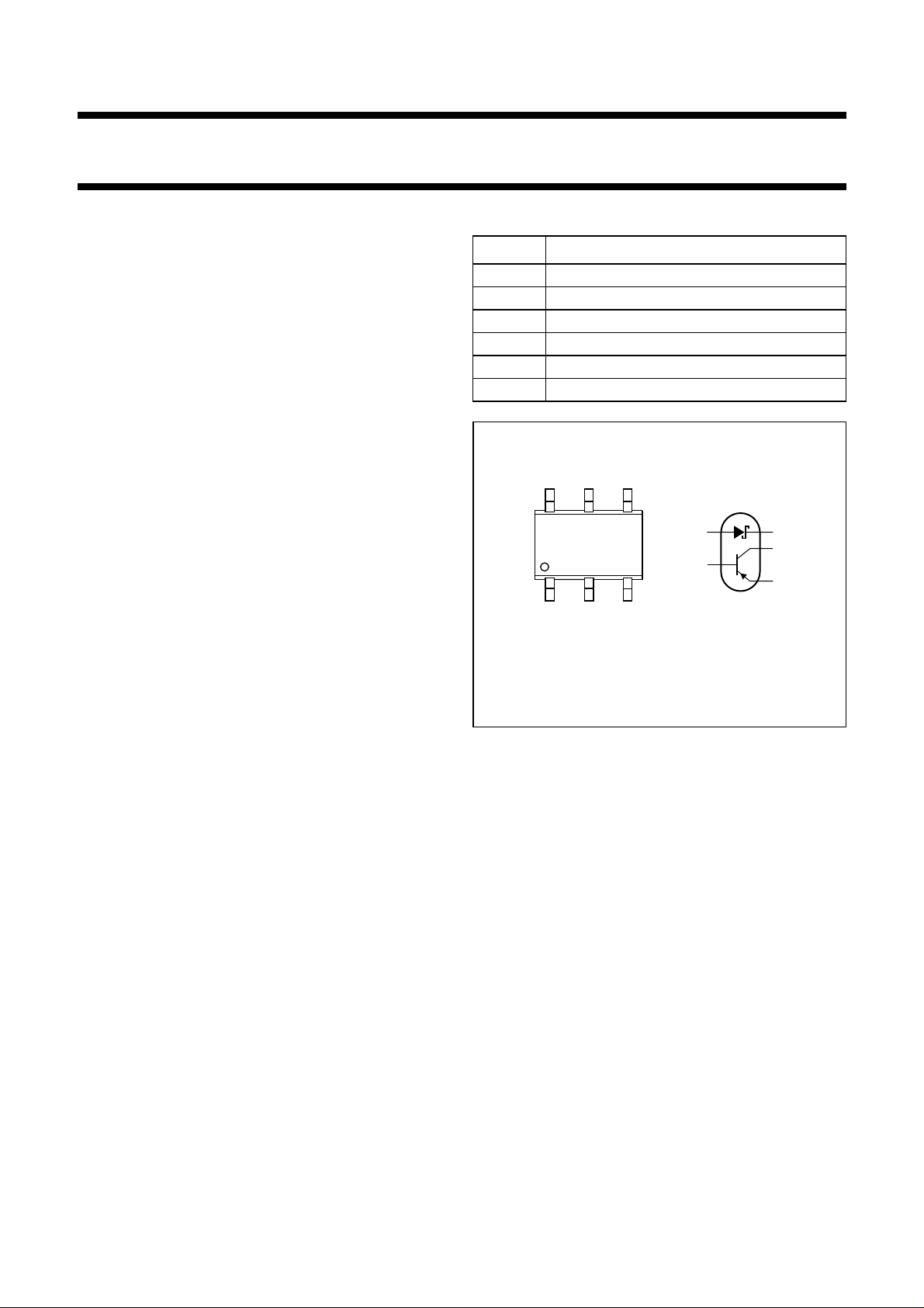
PINNING
PIN DESCRIPTION
1 emitter
2 not connected
3 cathode
4 anode
5 base
6 collector
handbook, halfpage
132
Marking code: B2.
56
4
4
5
MGU868
3
6
1
DESCRIPTION
Combination of a PNP transistor with low V
CEsat
and high
current capability anda planar Schottky barrier diode with
an integrated guard ring for stress protection in a SOT457
(SC-74) small plastic package.
NPN complement: PMEM4010ND.
Fig.1 Simplified outline (SOT457) and symbol.
2002 Oct 28 2

Philips Semiconductors Product specification
PNP transistor/Schottky diode module PMEM4010PD
LIMITING VALUES
In accordance with the Absolute Maximum Rating System (IEC 60134).
SYMBOL PARAMETER CONDITIONS MIN. MAX. UNIT
NPN transistor
V
CBO
V
CEO
V
EBO
I
C
I
CM
I
BM
T
j
Schottky barrier diode
V
R
I
F
I
FSM
T
j
Combined device
P
tot
T
stg
T
amb
collector-base voltage open emitter −−40 V
collector-emitter voltage open base −−40 V
emitter-base voltage open collector −−5V
collector current (DC) −−1A
peak collector current −−2A
peak base current −−1A
junction temperature − 150 °C
continuous reverse voltage − 20 V
continuous forward current − 1A
non repetitive peak forward current t = 8.3 ms half sinewave;
− 5A
JEDEC method
junction temperature − 125 °C
total power dissipation T
≤ 25 °C; note 1 − 600 mW
amb
storage temperature −65 +150 °C
operating ambient temperature −65 +125 °C
Note
1. Device mounted on a printed-circuit board; single sided copper; tinplated; mounting pad for collector 1 cm
THERMAL CHARACTERISTICS
SYMBOL PARAMETER CONDITIONS VALUE UNIT
R
th j-a
thermal resistance from junction to ambient in free air; note 1 208 K/W
Note
1. Device mounted on a printed-circuit board; single sided copper; tinplated; mounting pad for collector 1 cm
2
.
2
.
2002 Oct 28 3

Philips Semiconductors Product specification
PNP transistor/Schottky diode module PMEM4010PD
CHARACTERISTICS
T
=25°C unless otherwise specified.
amb
SYMBOL PARAMETER CONDITIONS MIN. TYP. MAX. UNIT
NPN transistor
I
CBO
I
CEO
I
EBO
h
FE
V
CEsat
V
BEsat
R
CEsat
V
BEon
f
T
Schottky barrier diode
V
F
I
R
C
d
collector-base cut-off current VCB= −40 V; IE=0 −−−100 nA
V
= −40 V; IE=0;
CB
T
= 150 °C
amb
−−−50 µA
collector-emitter cut-off current VCE= −30 V; IB=0 −−−100 nA
emitter-base cut-off current VEB= −5 V; IC=0 −−−100 nA
DC current gain VCE= −5 V; IC= −1 mA 300 −−
V
= −5 V; IC= −100 mA 300 − 800
CE
= −5 V; IC= −500 mA 250 −−
V
CE
V
= −5 V; IC= −1 A 160 −−
CE
collector-emitter saturation voltage IC= −100 mA; IB= −1mA −−−140 mV
I
= −500 mA; IB= −50 mA −−−170 mV
C
I
= −1 A; IB= −100 mA −−−310 mV
C
base-emitter saturation voltage IC= −1 A; IB= −50 mA −−−1.1 V
equivalent on-resistance IC= −500 mA; IB= −50 mA;
− 300 <340 mΩ
note 1
base-emitter turn-on voltage VCE= −5 V; IC= −1A −−−1V
transition frequency IC= −50 mA; VCE= −10 V;
150 −−MHz
f = 100 MHz
continuous forward voltage IF= 10 mA; note 1 − 240 270 mV
I
= 100 mA; note 1 − 300 350 mV
F
I
= 1000 mA; see Fig.7; note 1 − 480 550 mV
F
reverse current VR= 5 V; note 1 − 510µA
V
= 8 V; note 1 − 720µA
R
V
= 15 V; see Fig.8; note 1 − 10 50 µA
R
diode capacitance VR= 5 V; f = 1 MHz; see Fig.9 − 19 25 pF
Note
1. Pulse test: t
≤ 300 µs; δ≤0.02.
p
2002 Oct 28 4
 Loading...