Philips PMEGXX10BEA, PMEGXX10BEV Technical data

查询PMEG2010BEA供应商
DISCRETE SEMICONDUCTORS
DATA SH EET
PMEGXX10BEA;
PMEGXX10BEV
1 A very low V
barrier rectifier
Product specification
Supersedes data of 2004 Apr 02
MEGA Schottky
F
2004 Jun 14

Philips Semiconductors Product specification
1 A very low VF MEGA Schottky
barrier rectifier
FEATURES
• Forward current: 1 A
• Reverse voltages: 20 V, 30 V, 40 V
• Very low forward voltage
• Ultra small and very small plastic SMD package
• Power dissipation comparable to SOT23.
APPLICATIONS
• High efficiency DC-to-DC conversion
• Voltage clamping
• Protection circuits
• Low voltage rectification
• Blocking diodes
• Low power consumption applications.
DESCRIPTION
PMEGXX10BEA;
PMEGXX10BEV
QUICK REFERENCE DATA
SYMBOL PARAMETER MAX. UNIT
I
F
V
R
PINNING
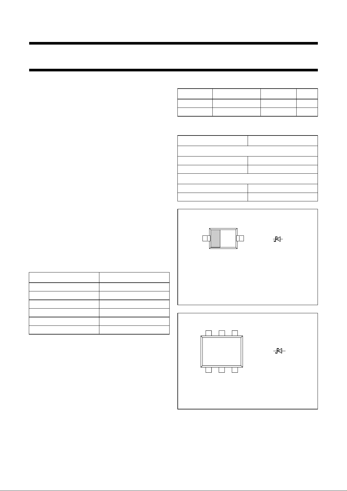
PMEGXX10BEA (see Fig.1)
PMEGXX10BEV (see Fig.2)
forward current 1 A
reverse voltage 20; 30; 40 V
PIN DESCRIPTION
1 cathode
2 anode
1, 2, 5, 6 cathode
3, 4 anode
Planar Maximum Efficiency General Application (MEGA)
Schottky barrier rectifier with an integrated guard ring for
stress protection, encapsulated in a very small SOD323
(SC-76) and ultra small SOT666 SMD plastic package.
MARKING
TYPE NUMBER MARKING CODE
PMEG2010BEA V1
PMEG3010BEA V2
PMEG4010BEA V3
PMEG2010BEV G6
PMEG3010BEV G5
PMEG4010BEV G4
21
12
Top view
The marking bar indicates the cathode.
sym001
Fig.1 Simplified outline (SOD323; SC-76) and
symbol.
5
46
1, 2
5, 6
123
Top view
3, 4
sym038
2004 Jun 14 2
Fig.2 Simplified outline (SOT666) and symbol.

Philips Semiconductors Product specification
1 A very low VF MEGA Schottky
barrier rectifier
ORDERING INFORMATION
TYPE NUMBER
PMEGXX10BEA − plastic surface mounted package; 2 leads SOD323
PMEGXX10BEV plastic surface mounted package; 6 leads SOT666
LIMITING VALUES
In accordance with the Absolute Maximum Rating System (IEC 60134).
SYMBOL PARAMETER CONDITIONS MIN. MAX. UNIT
V
R
I
F
I
FRM
I
FSM
T
j
T
amb
T
stg
NAME DESCRIPTION VERSION
continuous reverse voltage
PMEG2010BEA/PMEG2010BEV − 20 V
PMEG3010BEA/PMEG3010BEV − 30 V
PMEG4010BEA/PMEG4010BEV − 40 V
continuous forward current Ts≤ 55 °C; note 1 − 1A
repetitive peak forward current tp≤ 1 ms; δ≤0.5; note 2 − 3.5 A
non-repetitive peak forward current tp= 8 ms; square wave;
junction temperature note 3 − 150 °C
operating ambient temperature note 3 −65 +150 °C
storage temperature −65 +150 °C
PACKAGE
note 2
PMEGXX10BEA;
PMEGXX10BEV
− 10 A
Notes
1. Refer to SOD323 (SC-76) and SOT666 standard mounting conditions.
2. Only valid if pins 3 and 4 are connected in parallel (SOT666 package).
3. For Schottkybarrier diodes thermal runaway has to be considered, as in some applications the reverse power losses
PRarea significantpart ofthe totalpower losses. Nomogramsfor determiningthe reversepower lossesPRandI
rating will be available on request.
F(AV)
2004 Jun 14 3

Philips Semiconductors Product specification
1 A very low VF MEGA Schottky
barrier rectifier
PMEGXX10BEA;
PMEGXX10BEV
THERMAL CHARACTERISTICS
SYMBOL PARAMETER CONDITIONS VALUE UNIT
PMEGXX10BEA (SOD323)
R
R
th(j-a)
th(j-s)
thermal resistance from junction to
ambient
thermal resistance from junction to
in free air; notes 1 and 2 450 K/W
in free air; notes 2 and 3 210 K/W
note 4 90 K/W
soldering point
PMEGXX10BEV (SOT666)
R
R
th(j-a)
th(j-s)
thermal resistance from junction to
ambient
thermal resistance from junction to
in free air; notes 2 and 5 405 K/W
in free air; notes 2 and 6 215 K/W
note 4 80 K/W
soldering point
Notes
1. Refer to SOD323 (SC-76) standard mounting conditions.
2. For Schottky barrier diodes thermal runaway has to be considered, as in some applications the reverse power losses
PRarea significantpart ofthe totalpower losses. Nomogramsfor determiningthe reversepower lossesPRandI
F(AV)
rating will be available on request.
3. Device mounted on an FR4 printed-circuit board with copper clad 10 × 10 mm.
4. Solder point of cathode tab.
5. Refer to SOT666 standard mounting conditions.
6. Only valid if pins 3 and 4 are connected in parallel (SOT666 package).
CHARACTERISTICS
T
=25°C unless otherwise specified.
amb
SYMBOL PARAMETER CONDITIONS
V
F
forward voltage IF= 0.1 mA 90 130 90 130 95 130 mV
IF= 1 mA 150 190 150 200 155 210 mV
IF= 10 mA 210 240 215 250 220 270 mV
IF= 100 mA 280 330 285 340 295 350 mV
IF= 500 mA 355 390 380 430 420 470 mV
IF= 1000 mA 420 500 450 560 540 640 mV
I
R
continuousreverse
current
VR= 10 V; note 1 15 40 12 30 7 20 µA
VR= 20 V; note 1 40 200 −−−−µA
VR= 30 V; note 1 −−40 150 −−µA
VR= 40 V; note 1 −−−−30 100 µA
C
d
diode capacitance VR= 1 V; f = 1 MHz 66 80 55 70 43 50 pF
Note
1. Pulse test: t
≤ 300 µs; δ≤0.02.
p
PMEG2010BEA/
PMEG2010BEV
PMEG3010BEA/
PMEG3010BEV
PMEG4010BEA/
PMEG4010BEV
TYP. MAX. TYP. MAX. TYP. MAX.
UNIT
2004 Jun 14 4
 Loading...