

Philips PMEG2005AEA, PMEG3005AEA, PMEG4005AEA Technical data
查询PMEG2005AEA供应商
DISCRETE SEMICONDUCTORS
DATA SH EET
book, halfpage
M3D049
PMEG2005AEA; PMEG3005AEA;
PMEG4005AEA
Very low V
MEGA Schottky barrier
F
rectifiers
Product specification 2003 Aug 20
Philips Semiconductors Product specification
Very low VF MEGA
Schottky barrier rectifiers
FEATURES
• Very low forward voltage
• High surge current
• Very small plastic SMD package.
APPLICATIONS
• Low voltage rectification
• High efficiency DC/DC conversion
• Voltage clamping
• Inverse polarity protection
• Low power consumption applications.
DESCRIPTION
Planar Maximum Efficiency General Application (MEGA)
Schottky barrier rectifier with an integrated guard ring for
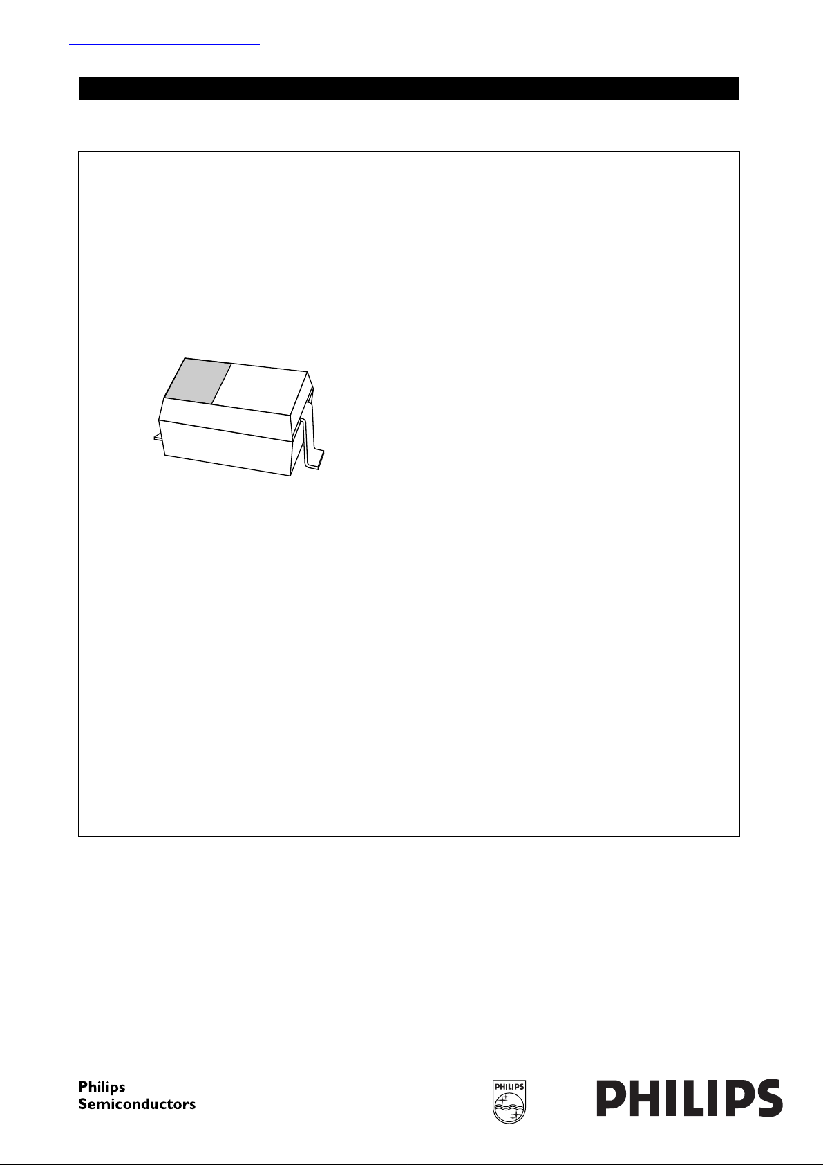
stressprotection,encapsulatedin aSOD323 (SC-76)very
small SMD plastic package.
PMEG2005AEA; PMEG3005AEA;
PMEG4005AEA
QUICK REFERENCE DATA
SYMBOL PARAMETER MAX. UNIT
I
F
V
R
PINNING
lumns
forward current 0.5 A
reverse voltage
PMEG2005AEA 20 V
PMEG3005AEA 30 V
PMEG4005AEA 40 V
PIN DESCRIPTION
1 cathode
2 anode
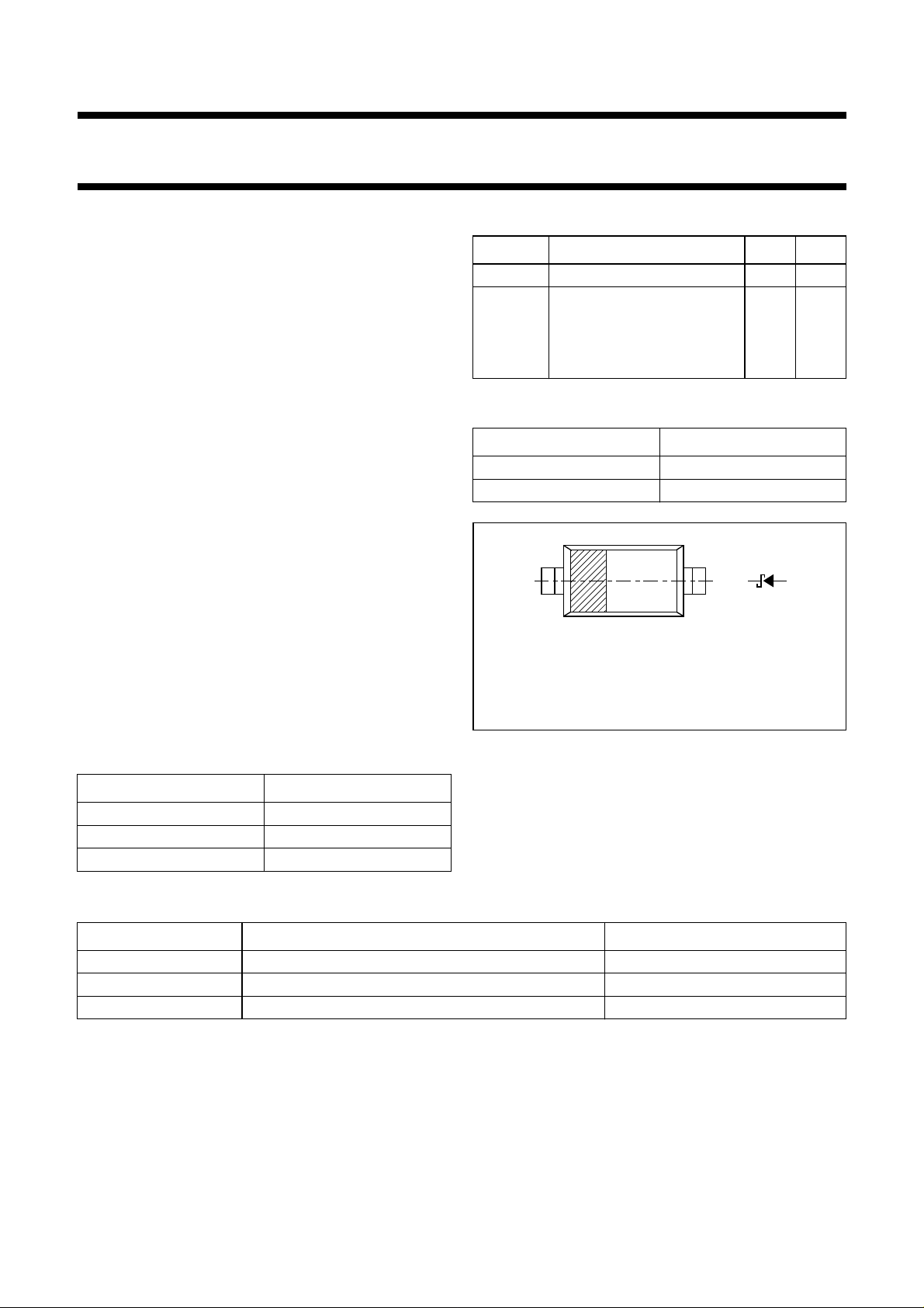
1
ka
2
The marking bar indicates the cathode.
Fig.1 Simplified outline (SOD323; SC-76) and
symbol.
MARKING
TYPE NUMBER MARKING CODE
PMEG2005AEA E5
PMEG3005AEA E4
PMEG4005AEA E3
RELATED PRODUCTS
TYPE NUMBER DESCRIPTION FEATURE
PMEGxx05AEV 0.5 A; 20/30/40 V very low V
PMEG2005EB 0.5 A; 20 V very low V
PMEG2010EA 1 A; 20 V very low V
F
MEGA Schottky rectifier higher forward current
F
MEGA Schottky rectifier SOT666 package
F
MEGA Schottky rectifier smaller SOD523 (SC-79) package
MAM283
2003 Aug 20 2

Philips Semiconductors Product specification
Very low VF MEGA
Schottky barrier rectifiers
PMEG2005AEA; PMEG3005AEA;
PMEG4005AEA
LIMITING VALUES
In accordance with the Absolute Maximum Rating System (IEC 60134).
SYMBOL PARAMETER CONDITIONS MIN. MAX. UNIT
V
R
continuous reverse voltage
PMEG2005AEA − 20 V
PMEG3005AEA − 30 V
PMEG4005AEA − 40 V
I
F
I
FRM
I
FSM
T
T
T
j
amb
stg
continuous forward current note 1 − 0.5 A
repetitive peak forward current tp≤ 1 ms; δ≤0.5 − 3.5 A
non-repetitive peak forward current tp= 8 ms; square wave − 10 A
junction temperature note 2 − 150 °C
operating ambient temperature note 2 −65 +150 °C
storage temperature −65 +150 °C
Notes
1. Refer to SOD323 (SC-76) standard mounting conditions.
2. For Schottkybarrier diodesthermal runawayhas to beconsidered, asin someapplications thereversepower losses
P
are asignificant part of thetotal power losses.Nomograms for determination ofthe reverse power lossesPRand
R
I
rating will be available on request.
F(AV)
THERMAL CHARACTERISTICS
SYMBOL PARAMETER CONDITIONS VALUE UNIT
R
R
th j-a
th j-s
thermal resistance from junction to
ambient
thermal resistance from junction to
in free air; notes 1 and 2 450 K/W
in free air; notes 2 and 3 210 K/W
note 4 90 K/W
soldering point
Notes
1. Refer to SOD323 (SC-76) standard mounting conditions.
2. For Schottkybarrier diodesthermal runawayhas to beconsidered, asin someapplications thereversepower losses
P
are asignificant part of thetotal power losses.Nomograms for determination ofthe reverse power lossesPRand
R
I
rating will be available on request.
F(AV)
3. Device mounted on an FR4 printed-circuit board with copper clad 10 × 10 mm.
4. Solder point of cathode tab.
2003 Aug 20 3
 Loading...