

Philips PMBF4391, PMBF4392, PMBF4393 Datasheet

DISCRETE SEMICONDUCTORS
DATA SH EET
PMBF4391; PMBF4392;
PMBF4393
N-channel FETs
Product specification
File under Discrete Semiconductors, SC07
April 1995
Philips Semiconductors Product specification
N-channel FETs
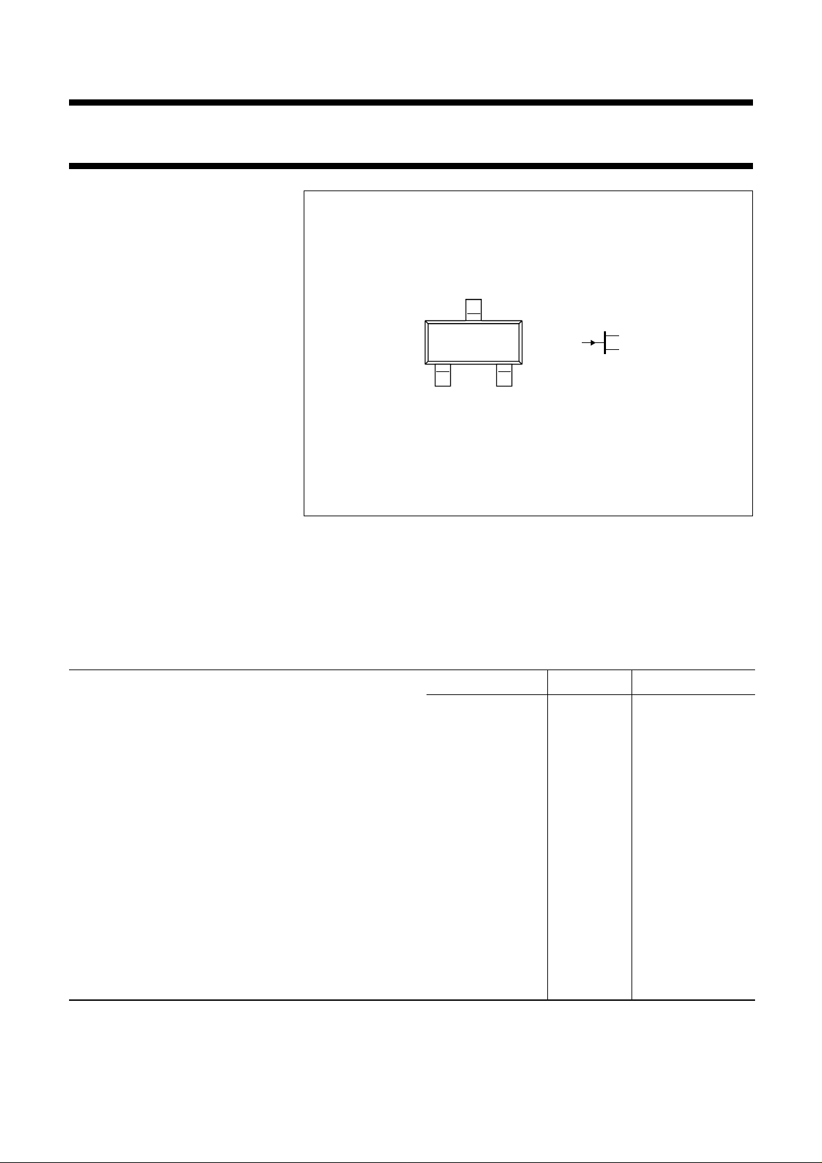
DESCRIPTION
Symmetrical silicon n-channel
depletion type junction field-effect
transistors on a plastic
microminiature envelope intended for
application in thick and thin-film
circuits. The transistors are intended
for low-power chopper or switching
applications in industry.
PINNING
1 = drain
2 = source
3 = gate
Note
1. Drain and source are
interchangeable.
PMBF4392; PMBF4393
handbook, halfpage
12
Top view
Fig.1 Simplified outline and symbol, SOT23.
3
g
MAM385
PMBF4391;
d
s
Marking code
PMBF4391 = p6J
PMBF4392 = p6K
PMBF4393 = p6G
QUICK REFERENCE DATA
Drain-source voltage ± V
Drain current
VDS= 20 V; VGS=0 I
Gate-source cut-off voltage
V
= 20 V; ID= 1 nA −V
DS
Drain-source resistance (on) at f = 1 kHz
I
= 0; VGS=0 R
D
Feedback capacitance at f = 1 MHz
−V
= 12 V; VDS=0 C
GS
Turn-off time
VDD= 10 V; VGS=0
= 12 mA; −V
I
D
I
= 6 mA; −V
D
= 3 mA; −V
I
D
= 12 V t
GSM
= 7 V t
GSM
= 5 V t
GSM
DSS
ds on
rs
off
off
off
DS
(P)GS
PMBF4391 PMBF4392 PMBF4393
max. 40 40 40 V
> 50 25 5 mA
> 4 2 0.5 V
< 10 5 3 V
< 30 60 100 Ω
< 3.5 3.5 3.5 pF
< 20 −−ns
<−35 − ns
<−−50 ns
April 1995 2
Philips Semiconductors Product specification
N-channel FETs
RATINGS
Limiting values in accordance with the Absolute Maximum System (IEC 134)
Drain-source voltage ± V
Drain-gate voltage V
Gate-source voltage −V
Gate current (DC) I
Total power dissipation up to T
amb
=40°C
(1)
Storage temperature range T
Junction temperature T
THERMAL RESISTANCE
From junction to ambient
(1)
CHARACTERISTICS
=25°C unless otherwise specified
T
j
Gate-source voltage
= 1 mA; VDS= 0 V
I
G
Gate-source cut-off current
V
= 0 V; −VGS= 20 V −I
DS
V
= 0 V; −VGS= 20 V; T
DS
= 150 °C −I
amb
Drain current
= 20 V; VGS=0 I
V
DS
DSS
DGO
GSO
G
P
tot
stg
j
R
th j-a
PMBF4391 PMBF4392 PMBF4393
>
<
PMBF4391; PMBF4392;
PMBF4393
DS
GSon
GSS
GSS
50
150
max. 40 V
max. 40 V
max. 40 V
max. 50 mA
max. 250 mW
−65 to + 150 °C
max. 150 °C
= 430 K/W
< 1V
< 0.1 nA
< 0.2 µA
25
75
530mA
mA
Gate-source breakdown voltage
−IG=1µA; VDS=0 −V
Gate-source cut-off voltage
I
= 1 nA; VDS= 20 V −V
D
Drain-source voltage (on)
ID= 12 mA; VGS=0 V
I
= 6 mA; VGS=0 V
D
I
= 3 mA; VGS=0 V
D
DSon
DSon
DSon
Drain-source resistance (on)
I
= 0; VGS= 0; f = 1 kHz; T
D
=25°Cr
amb
ds on
Drain cut-off current
−VGS= 12 V
−V
=7 V I
GS
−V
=5 V I
GS
= 12 V
−V
GS
=7 V I
−V
GS
−V
=5 V I
GS
V
DS
V
DS
= 20 V
= 20 V; T
amb
= 150 °C
I
DSX
DSX
DSX
I
DSX
DSX
DSX
April 1995 3
(BR)GSS
(P)GS
> 40 40 40 V
>
<
10
4
250.53V
V
< 0.4 −−V
< 0.4 − V
<− −0.4 V
< 30 − 100 Ω
< 0.1 −−nA
<− 0.1 − nA
<− −0.1 nA
< 0.2 −−µA
<− 0.2 −µA
<− −0.2 µA
 Loading...