

Philips PMBF170 Datasheet

DISCRETE SEMICONDUCTORS
DATA SH EET
PMBF170
N-channel enhancement mode
vertical D-MOS transistor
Product specification
File under Discrete Semiconductors, SC13b
April 1995
Philips Semiconductors Product specification
N-channel enhancement mode vertical
D-MOS transistor
DESCRIPTION
N-channel enhancement mode
vertical D-MOS transistor in a SOT23
envelope. Designed for use as a
Surface Mounted Device (SMD) in
thin and thick-film circuits with
applications in relay, high-speed and
line transformer drivers.
FEATURES
• Direct interface to C-MOS, TTL,
etc.
• High-speed switching
• No secondary breakdown
QUICK REFERENCE DATA
Drain-source voltage V
Gate-source voltage (open drain) ± V
Drain current (DC) I
Total power dissipation up
to T
=25°CP
amb
Drain-source on-resistance
I
= 200 mA; VGS=10V
D
Transfer admittance
I
= 200 mA; VDS=10V
D
PINNING - SOT23
1 = gate
2 = source
3 = drain
Marking code:
DS
D
tot
R
DS(on)
| Yfs|
PMBF170
max. 60 V
max. 20 V
GSO
max. 250 mA
max. 300 mW
typ.
max.
min.
typ.
2.5
5.0ΩΩ
100
200mSmS
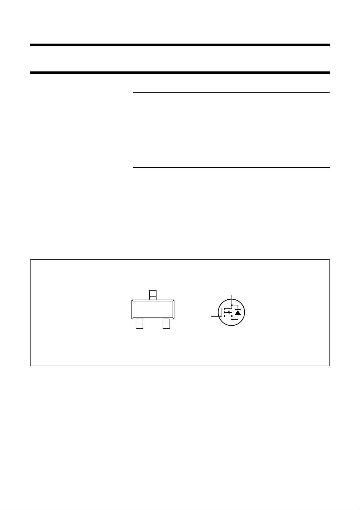
PIN CONFIGURATION
handbook, halfpage
PMBF170 =
12
Top view
PKX
3
MSB003
handbook, 2 columns
g
MBB076 - 1
Fig.1 Simplified outline and symbol.
d
s
April 1995 2

Philips Semiconductors Product specification
N-channel enhancement mode vertical
D-MOS transistor
RATINGS
Limiting values in accordance with the Absolute Maximum System (IEC 134)
Drain-source voltage V
Gate-source voltage (open drain) ± V
Drain current (DC) I
Drain current (peak) I
Total power dissipation up to
=25°C (note 1) P
T
amb
Storage temperature range T
Junction temperature T
THERMAL RESISTANCE
From junction to ambient (note 1) R
From junction to ambient (note 2) R
Notes
1. Mounted on ceramic substrate measuring 10 mm × 8mm ×0.7 mm.
2. Mounted on printed-circuit board.
DS
D
DM
tot
stg
j
th j-a
th j-a
GSO
PMBF170
max. 60 V
max. 20 V
max. 250 mA
max. 500 mA
max.
max.
−65 to +150 °C
max. 150 °C
= 430 K/W
= 500 K/W
300
250
mW (note 1)
mW (note 2)
April 1995 3
 Loading...