

Page 1

GI
sd
Automatic Digital
PM
PM
Service Manual
9499 475
790507
2517E ,,o,onu
2517X o,0,.0.,
01311
Multimeter
l
l
l
rO
l
l
l
I
l
l
I
)
PHITIPS
l
Page 2

PHITIPS
equipment
e
for
$EmUrcE***fil
79 06 06
AIreodY issued:
Re :
-
Documentotion
D ocume
lnstruction
nto tion
su
mqnuol
version of OQ
New
rvey
lnstrument
9499
PM 2517E/X
versions
475 01011
0063
E DMO]
DMol 600
X
E
600
DM02
X DM0l 3051
and
-
D M02 4926
-
DMO] 3051
4926 - onwords
science
industry
-
onwords
SME
83
475
lnstruction
Service
-
New version of OQ
In
Using
(E
of
some.
To
using
noie
the
new
ihe
DMOI 600
the
Q-function.
Concern Service
qvoid
them in the eorlier
mqnuql 9499
SME 83
0063
version of
new
OQ
-
problems
the OQ 0063
0063
D MO2
4926 ond
The ordering
with
in ihe eorlier
willdeliver only
the
01311
X DM 0l 600
number of
Q-function,
PM 2517.
'17
pin
versions of
lhe new
pin
is internolly connected.
the PM 2512
-
DM0l 3051)
the OQ 0063,
version of
the
l7 of
OQ
results
209 85886
5322
the OQ 0063.
should be
0063
in molfunctionning
remoins
cut-off
the
when
I
I
I
9499
478
09511
J
J
Page 3

il
t
t
oQ 0063
old
DM0l 600 - DM02
-
DM01 600
DMOI
4926
3051
New OQ
M02 4926 - onwords
D
DM0l
3051
0063
-
onwords
T----1
--
=-
I
t
Ij
ll
oo
(
oLD
0063
BOARD
PC.
0063
oo
(
)
NEw P.C. BOARD
sr
)
I
2717
Page 4

PHITIPS
equipment
800218
le
for
$EHUIGE****m
PM2s17
Alreody
Re
L
Storting
-
.
-
issued r SME
:
: 2. Botiery
: 3.
:
problems
descript ion
Error
the PM251/ is
lf
it moy hoppen thot the
-
-
In both
ON
correctly ogcr
Couse
Storting
The
coses fhe PM251Z does not reoct
ogoin or to the functions
problems
problem
83
1.
Storiing
Predeflecfion
4. lncorrect reoding
OQ0063
Disploy
Disploy
in.
only occurs
problems
cover
in the
.
switched-on
OQ0063
indicotes overlood
indicotes o too low reoding
of the OQ0063.
with new LC.
E/X
OQ00l,3
=':=
mA
the mA ronges
in
the function
in
does not storf.
V=, Vn , mA==or mArw
ronge
Q,
on ronge commonds.
's
with
or
d
This con result in
weeknumberT9l9 ond higher
and industry
oC
*ith
the instrument functions
science
op.n input or
the
following
After
switching
SMEB4
Rx
8000,
errors:
OFF
(refer
ond
to
sME 83).
-
Remedy
PM25I7E
PM2stTX
DMOI 600 - DM02 4926
DM01 600 - DM0l
3051
when
Only
modificotion must
the OQ0063 is reploced
-
Remove copocitor
-
Short circuit resistor R4l3
-
Connect to
copocitor
10
be built- in:
pin lZ
l5
of
(pin
lZ
15
17 18
by
C407
ond pin l5
10V in
PF,
of the
o new type
(22nF
\
(3k3)
($
porollel
OQ0063 should be cut
(weeknumber
of the
)
R4l8
c407- 1+
OQ0063
with o resistor of
=
68 kO,
F
l
'-79.19)
on electrolytic
off, refer to SME83).
CRl6 5322
10V
,
the following
kQ, CR16.
68
l l r
s322 124
9499
30291
t4036
478 10811
l
Page 5

2517E
PM
PM25\7X
-
DM 02
DM 0r 3051 - DM 04 86il
4926
DM 04
10491
t"
t;
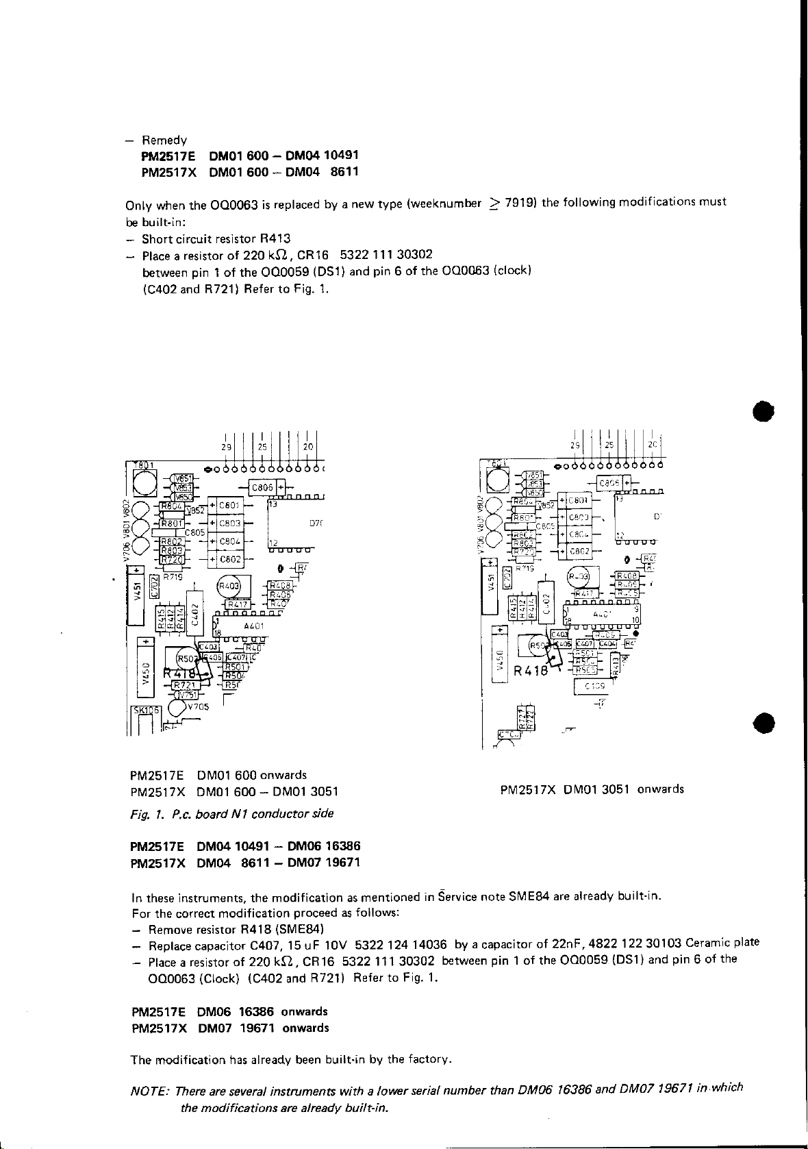
lf the OQ0063 hos q weeknumber of7919or higher the following
c404
F---n
R
413
fr
T
Connect to
15P F in porollel with o
Proceed
-
Remove
-
Remove
-
Remove resistor R413
-
Short circuii the spots
-
Mounl copocitor C404 on the
-
Mount the new
c401
pin l/
os
follows:
copocitor C407
copociior C404
c404
F-l
OLD
of the OQ0063
resistor of 68
copocitor
15uF
wrres in
clrcurr
short
NNODIFIED
cne
-
(3k3)
where R4l3 hqs been removed
Mount fhe 68 kQ resistor befween
OO0063
ond
supply
kQ ond
(22nF
)
(1nF)
p.c.
(15 p
C407
R4lB R= 68
C407
hole
ot the conductor side of the
zero $ on electrolytic copocitor
short
ogoin.
boord
f)on the
C=l5p
modificotion must be built in,
circuif
p.c.
ka, CRl6 5322
F, 10V
resistor R413.
(see
figure)
boord
5322
pin
ogoin
(see
lll
30291
124 14036
15 ond lZ
p.c.
boord.
figure) '
of
of the
I
t,.,
[,
r'
I
:r
I
a
Ir
5;
r;
[1
CURRENT SOURCE
t;
r;
r,
-l:,.
I
:r
PM 2517E
PM
2517X DM04 8611
DM04
The
modificqtion
10491
hos
-
onwqrds
-
onwords
olreody been built
in from the foctory
on.
tJ
Page 6

I
.l
1
I
l
J
I
J
l
erratum lor
"oncerns:l. Starting
polarity
The
circuitdiagram
SME
of
the
must be
84 code
new
nr 9499 478
problems
000063
capacitor C407
changed to show; Pin
10811.
is drawn incorrectly.The
17 of the 000063
pin
15 of the 000063
drawing
(4401) = _
(A4ot) =
of the l.C, and the
(+)
+
Page 7

2. Botte rycove r.
3.
Sofety requirements mode it necessory thot the
meosured on should be
Therefore the
bottery spring ond the bottery cover
The ordering number
bottery cover is reploced olso the
ploced
the
of
lower.
bottery cover reomoins
bottery spring should be
bottery spring
Description Orde ri ng number Qtv.
Bottery
Bottery
Predeflection
-
Error descript ion
ln
-
Remedy
Cut trock which is situoted
boord
Interconnect pin24
From
on the modificotion hos olreody
cover 5322 443
spring
low
in the mA:=: ronge.
the mA
-- ronge the PM 251 Z hqs o
(see
figure).
number DM 06 15321
seriql
64026
5322 492 64746
the
under
the
of
OQ0059
PM2517E ond
been built in
predeflection
OQ0064
(D101)
ond
(lorger
the
some. In ol
(A102)
pin
7
DM 06
the
by
where the
hole) hove
d instruments where the
reploced.
of
2 digits of
ot the
of
conducior side of
the
OQ0060
14986
foctory.
boftery
voltoge is
been chonged.
shortcircuited
(Al0l) (see
PM2517X
input.
the
figure)
p.c.
WIRE
4.
---
Incorrect reoding
-
Error desc ription
High
current
mA ronge.
-
Remedy
A new
in the
resistor
mA ronges.
peoks
This will give
type R603,
con influence permonently
o permonent
ordering
incorrect reoding.
number
5322
CUT
TRACK
the
volue of resistor R603
ll6 44011.
in the
Page 8

PHITIPS
equipment
for
science
$EmUilGE*d**ffi
800408
Already
Re:
issued: Sl\4 E
st\4E
New
-
Documentation
lnstruction
83
84
LX display
survey
manual
9499 475 010'1
PM
2517X
E
DM01
600 - Ot\402 4926
x Dt\40'l
E DI\402
1
-
DM01
600
4926 ONWAB DS
x DM01
X DI\407
and industry
SME 85
305'|
3051 - Dr\407 17361
17361 ONWARDS
lo
Instruction
Service note
New
l.
LX displav
From
serial number DM
and lrom
LX display
The new
In
addition
pin
Nl
manual
serial number
{height)
rubber
interconnection
to the new
3.
9499 475
SME 83
SME
84
SME
85
07 17361
DM 07
differ from
LX display
0'1311
onwards
19138 with
the
excisting display.
strip has
a wire
been
is soldered between
pM2571X
the
a new rubber interconnection
mounted, to ease the
is equipped
the soldering bulb
with a new
strip.
mounting.
LX disptay
The dimensions
on the LX display
(type
of the new
BBC)
and
9499 478
10911
Page 9

OLD
PM2517X
LX display
1=
F
lexible interconnection
2=
Ru bber
3=
Tape
4=
5= Large
Display
6=
Fixing
7=
Positioning hook
8=
DM0r
(5322
roller
fixing clip
unit
2x
clip
SITUATION
-
Dl\,107 17361
600
130 94011
strip
obsolete)
sT 2541
PM2517X D
LX display
1=
Flexible rubber
2=
263 540141
15322
5= Large
6=
7= Fixing clip
8=
fixing clip
Display unit
Positioning
NEW
SITUATION
l\.407
(5322
130 94025)
interconnection
2x
hook
'19138
strip
onwards
In
new arrangement
the
page
1l2 of
How to
2-
The existing
when
For
replace
Ordering numbers,
3.
Obsolete until oresent
LX DTSPLAY
Plvl2517Instruction
the
proceed
LX display 532213O
display has to be
LX
the
refer to
rubber roller
the
lvlanual.
with old instruments
9401 1 is
replaced, the existing
page
112 of the
stocks are exhausted
(3)
and tape
(PM2517X
obsolete
PM25l7
AODITIONAL
BETWEEN SOLOERING
THE
ON
N1 PIN 3
(4)
are not required.
600
-
DMOT 1
DM0l
interconnection strip
instruction manual and
5322 130 9401 1
7361)
WIRE
LX OI5PLAY
To replace the
be
also
should
point
1 of this
zoos
sr
LX display.
replaced.
information
refer
sheet.
I
to
Replaced
LX
Rubber interconnection strip
by
DISPLAY
(Type
B BC)
5322 130 94025
5322 263 54014
Page 10

PHI[IPS
.']
I
I
equipment
I
for
science
$EMUilGEnfi**ffi
801009
I
J
Already
Rc :
Documentation
issued:
1.
Starting
2. ON/STAND
Textplates
3.
4.
Corrections
Survey
SME83,
problems
of the
SME84,
000063
BY/OFF
Service manual
Sl\4885.
switch PM2517E
PM2517
E.
DM
0't
x
DMor
ElX
-
600
600 - Dt\401
Dt\402
4926
x
DM01
x DM07
DM06
DM02
4
3051
-
DM06 16386
3051 - DM07
-
17361
X Dl\407
16383
19671
DM07
onwards
and industry
SME87
17361
19671
onwards
Instruction
Instruction
Service note
Starting
The remedy
sufficient.
It
-
-
probl€ms
should be
Error
descriotion
lf
the PNr2517
it
may happen
-
-
In both
ON again
correctly agäin.
Cause
Starting
The
cases the Plvl2517 does
problems
problem
manual
manual
9499 475
9499 475
SME83
st\4E84
SME85
SME87
000063.
for
the
starting
replaced
is
switched-on
that
Display indicates
Display
indicates
or to the functions
only occu
problems
by the remedy
the 000063
of the
O00063
rs with
01Ol1
0131'l
as described
in
the function
does
overload
a too low
not react
V=,
new r.c.'s
of the
currentsource
not
start. This
reading
on
Vrv,
mA:=or
with
000063
in
this
Service note.
Sl,, I o,
range
weeknumber
oC
can result in
commands. After
mA.\.,/the
with
7919
open input
instrument
as described
the followinq
switching OFF
higher
and
in
o, Rx )
functions
(refer
Service note
800 f,2
errors:
and
to sMEg3).
9499 478 11111
SlVEg4.
,
is not
Page 11
-
Remedy
PM2517E
PM2517X DM01 600-
DM01
600- DMO4
DM04
10491
8611
when
Onlv
built-in:
be
-
Short circuit
-
Place a
between
(C402
OQOO63
the
resistor
resistor of 220
pin
1 of the OOOO59
Refer to
R721)
and
replaced by a
is
R413
ksr. cR16
{DS1)
Fig.
new type
532211130302
pin
and
1
(w€eknumber
of the 000063
6
7919)
>
(clock)
following modifications
the
must
PM25l7E
PM2517X Dt\401
Fig. l.
PM2517E DM04
PM2517X DM04
In these instruments, the
For
the correct
-
Remove resistor
-
Replace capacitor
place
000063
PM2517E DM06
PM2517X
The modification
NOTE: There
D l\401
600
-
600
P.c,
board
Nl
conductor
10491 - DM06
8611
modification
R418
C407, 15uF 1OV
a resistor
the modifications are alreadv built-in,
of 220
(Clock)
DM07
lC4O2
16386 onwards
19671 onwards
has already been built-in
are several instruments
onwards
DM01 3051
side
16386
-
DM07 19671
modification as mentioned
proceed
(SME84)
kS)
,
and
as follows:
5322 11 I 30302
CR16
R721)
Referto
with a lower
5322124
by the
Plvl2s17X
in Service note SME84
14036
Fig. 1.
factory.
serial
by a
capacitor
b€tw€en
number than DMO6
pin
l\4O
D
l 3051
are already
of 22nF,4822122
1 of the OO0059
and
16386
onwards
built'in.
30103
(DS1)
DM07 19671
and
pin
Ceramic
the
of
6
which
in
plate
Page 12

2.
ON/STAND BY/OFF
switch PM2517E
J.
an
The lockspring,
switching. The
The
new ordering
Lockspring
Ball
bearing
Textolates
To conform with
The ordering numbers
Topcover
Baftervcover E/X
Topcover
Corrections of the
Page
65 5.2. Adjusting
X
5322
topcover
numLlers
5322 492
4822 52O 4OO12
the international
5322 447
5322 443 64029
5322 447
Service manual
NO.2 ADJUSTING
Adj. resistor R'107
lMR25,
492
part
64675,
now
are:
power
of
the
consists of a
switch in the topcover has been
locking-spring,
64742
standards, the text on
for
the topcover and bafterycover with
94558
94537
table
1'Ä, E48
(ordering
series)
number
E LEMENT
9499 475 0131 1)
modified to ensure
two ball bearings
the topcover and the batterycover has been modified.
new
the
texts are:
and a
knob.
a smooth
Should be Adj. resistor
changed into:
'
Adjustment
NO.1'l
lMR25,
Potentiometer
1o/., E48
must be omitted
R107,
coarse.
series)
R 106, fine.
Page 13

CONTENTS
Pt:A 2517E
Page
3
1.
1.1.
1 .2.
t.J.
2.
2.1 .
2.2.
J.
3.2.
3.3.
3.4.
4.
4.2.
4.3.
5.
5.2.
TECHN ICAL
Electrical specifications
General
Power
supply
ACCESSOR tES
Accessories supplied
Optional accessories
CIRCUIT DESCR
General
Principle of operation
Detailed circuit description
Specifications of !C's used in the
ACCES
General
Dismantling
Replacing
ECKING AND AOJUSTING
CH
General
Adjusting
DATA
data
with rechargeable
with
IPTION
PM 2517
the
parts
table
instrument
the
batteries
Pl\il
2517
5
5
7
8
I
I
I
16
to
20
41
60
60
60
60
64
64
65
.3.
2517
TROUBLE
Power
Ranging
A-ranges
A-
ranges
oC
range
if
range
Modif
X
SHOOTING
supply
LIST,
ications in rhe P[i]
6.
6.1.
6.2. Display
6.3. ADC
6.4. V-attenuator
6.5.
6.6. V- ranges
6.7. f,2 ranges
6.8.
6,9.
6.10.
6.11.
6.12. Stand-by
6.13. Data hold
7. PABTS
1 .1. lvlechanical
7 -2. Electrical
1
Prlr
2517E
61
69
10
12
75
76
78
81
82
83
84
84
84
85
86
86
88
92
105
Page 14

IMPORTANT
ln correspondence concerning this
plate.
type
WICHTIG
8ei Schriftwechsel über
anzugeben. Diese be{inden sich auf
IMPORTANT
dieses Gerät wird
please
instrument,
gebeten,
dem Leistungsschild.
quote
genaue
die
the tVpe
number
Typenbezeichnung
and
serial
die
und
number
Gerätenummer
given
as
on the
rl
[,
[.'_
t
t
t
RECHANGE DES
Dans votre correspondance et
le num6ro de type et le num610
Note.
PIECES DETACHEES
dans vos r6clamations
de s6rie
The
Consequently, this instrument may
contained in this manual.
design
of
this
(R6parations)
se rapportant ä
quisont
instrument is sublect to continuous development and
marqu6s sur
incorporate
cet appareil, veuillez
plaquette
la
minor changes
de caract6ristiques.
in
detail
TOUJOURS
imprcvement.
from
information
the
indiquer
t
?
Bemerkung:
Remarques:
@ N.V.
Die Konstruktion und Schaltung dieses Geräts wird ständig weiteren twickelt und verbessert.
Deswegen kann dieses Gerdt von cien in dieser Anleitung stehenden Angaben abweichen.
Cet appareil est
certains dötails
d'emploi et
PHILIPS'
GLOEILAMPENFABRIEKEN
l'objet
mineuß
d'entretien.
de d6veloppemens et amöliorctions continuels.
peuvent
difförer des informations
_
EINDHOVEN
_
donn6es dans
THE
En
consöquence.
pr6sente
la
NETHERLANDS
notice
_
[,
q
+
r
1979
I
Page 15

l
l
l
l
j
l
l
l
I
,o
l
l
PHITIPS
5T
233(
l
j
l
l
jo
l
)
.l
Service
Automatic
Manual
Digital
PM2517E
9441 625 11O.1
From
serial
number
Dl\,4 02
4926
onwards
Multimeter
l
I
475
9499
01311
Page 16

4
LIST OF
FIGURES
Page
L
r
t-|
r
-
L
2.
3.
4.
5.
6.
7.
8.
9.
10.
11.
12.
13.
to.
17.
18.
19.
20.
21.
22.
23.
24.
25.
26.
27.
28..
29.
30.
32.
33.
34.
35.
36.
37.
38.
39.
40.
42.
43.
45.
46.
47.
48.
49.
50.
51.
52.
53.
54.
Power
supply
Temperature
Data hold
probe
H F
Accessory
probe
R.F.
probe
EHT
Current transformer
Shunt
Block
Basic built up of Pl\tl 2517E
D.c. voltage measurements
A.c. voltage measurements
D.c. current measurements
A.c.
current measurements
Resistance measurements
Compensation
Protection
Temperature measurements
ADC
Data signals examples
BIock diagram of digital section
Flow
chart and
Pulse
diaqram of UP/DOWN/AUT ranging
Timing
Power
Pinning HEF
lock diagram HEF
B
LED indication
Pinning HEF
B lock diagram
Pinning
Pinning
B lock diagram OO 0059
Pinning
Pinning
Pinning
Pinning
D ismantling
Inside
Inside view
Mounting the
10A switch
Adjusting
Faultf
Inside view of
Bottom cover with item numbers
Input block with item numbers
P.c.
board with item numbers
P.c. boards component
P.c. boards
Function
Survey of used components in the
Circuit diagram
probe
Pl\.4
9248
probe
PM 9263
PM
921 0
PN4
set
9212
PlVl 9213
PM
9246
Plvl
9245
PlVl
9244
d iagram PM
resistance ranges
of display unil
supply signals
and block diagram of OO
OO
and block
and block diagram OO
and block diagram OO
and block diagram OO 0064
view
top
elements
inding block
conductor
switch lay'out
2517E
ADC
of
tim ing
451 1B
45558
HEF
0059
the
on
of top cover
power
top
current
45118
45558
diagram OO 0060
Plvl
2517
p.c.
board
switch knob
diagram
cover with item numbers
PIM
side
Pl\4 2517E
side
PM
2517E
0061
0063
2517E
0055
PNI 2517
10
14
14
14
14
13
14
14
14
18
20
20
22
25
25
27
27
27
28
31
29
32
33
39
40
41
41
43
43
44
4B
48
52
54
56
5B
62
62
62
61
62
64
66
87
87
81
B7
95
96
91
98
101
t".1
r'
Ll
r
I
Ll
t_
r
ö
t
t_
i:
r'
I
-l
t-
t
?
t
tt
t:
I
Page 17

l
-l
l
I
J
-.l
I
l
l
l
l
I
I
)
l
I
J
I
I
I
.,
1.1. ELECTRICAL
1.1.1, D.C.
1.1.2
rEcHNrcAL
All values
by
Range
Resolution
Accuracy
Temperature
Input impedance
Protected
A.C.
Range
.
R esolution
AccuracV
Frequency
Temperature
lnput impedance
mentioned
the manucfacturer.
voltage measurements
up to
voltage measurements
influence
coefficient
coeff icient
DArA
in this description
SPECIFICATIONS
4 sub-ranges:
Additional
4O
'10
300
Range
999.9 mV
9.999
are nominal;
100
irv
4 sub ranges:
100
!V
t
0.29,"
ppm/oC
300
Range
999.9 mV
9.999 V
99.99 V
999.9 V
1000V...
1400 V
100pV...
100sV
i
0.57o of reading
Valid
H2...
1 kHz..
kHz..
ppm/oC
'1000
. . .
999.9 mV:9.999
reading
of
of readinq
or 1000 V^-
peak
1000
999.9 mV;9.999
) 1% of range
error
Error
l kHz
. 10 kHz
.20 kHz
of reading
V
those
V
10
05%
Input
10 t\ro
I tvl
V
10.1%
t
7o
Input
2Mf,2
given
with
full
of
impedance
1
1%
01 I 19l"
rms
full
of
full
of
scale
t1
+q
impedance
x17.
tolerances
V;99.99 V;999.9
scale
V;99.99 V;999.9
scale
are binding and
(50H2)
guaranteed
V
V
,]
l
I
I
l
l
AC-DC
Crest factor
Protected
conversion
up
to
99.99
V
999.9
V
True
R lvls
2 at
end
of range
600 V-
1400 V peak
rms
+
400
t\,
1
V:-:.:
802
J
1%
Page 18

6
1.1.3.
1 .1.4.
D.C.
cu.rrent
Range
Resolution
Accuracy
Temperature
Voltage
Protected
A.C.
Range
drop
up to
current
measurements
measurements
coeff
icient
over
shunt
-
10/lA
l mA-
2
t
0.570 of reading
500
Range
99.99
9.999
Range
99.99 mA
9.999 A
10
I mA'
2 fixed ranges
fixed
ppm/oC
A
.
100 mA
!A
100
mA
10A
ranges
of
104
with
separate inputs;
10.'l%
reading
Voltage
(
200
(
150 mV
Protection
Fuse
315 mA
protectron
No
with
separate
of full
scale
drop
mV
quick
inputs;99.99
99.99
9.999 A
9.999 A
mA
250 V rms
mA
Resolution
Accuracy
Temperature
Voltage
Protected
1.1.5. Rssistanc€measurements
Range
Resolution
Accuracy
drop
up to
coef f icient
over
shunt
Range
99.99 mA
9.999
A
i
0.8%
of reading
ppm/oC
500
Range
99.99 mA
9.999
A
Range
99.99
mA
9.999
A
0.1 Q....10tvo
5
sub-ranges:
10.19,"
of reading
999.9
999.9
0.1 r,
Range t
999.9
9.999 kQ
99.99
999.9 kO
9.999 tvlQ
s2
kO
R
eso lu
tio n
10
llA
of
full scale
Voltage
(
<
Protection
Fuse
No
Q ; 9.999
kO;9.999
drop
200
mV
150
mV
mA quick
315
protection
7o of reading
r
0.5
t
1
kQ
M O
at
50 Hz
;99.99
1
% of fult
250 V rms
kQ
r
0.1
10.1
input
scate
signal
Page 19

'l
I
J
Temperature
I
Protected
up
coef
to
f icient
Range Temp. coefficient
999.9 5l
9.999 kO
99.99
999.9 kf,,
kQ
9.999 tvl Q
250 V
rms
300
500
ppm/oC
ppm/oC
of reading
reading
of
I
J
I
'
I
I
I
r.r.o. Diode
_..
unvtng
Ranse
P rotected
1.1-7.
'.r.
Temperature
Probe
to
l\4easuring
Accuracy
(Probe
GENERAL
D isplay
Maximum
Overrange indication
Polarity
Unit indication
Function
Inputs
Rang€
selection
Series mode
(SM
RR) dc ranges
Common
(C|\4RR)
Analog
Conversion
Conversion
Protection
measurements
current
up to
measurements
be used
range
combined with
PM
DArA
reading
indication
indication
rejection ratio
mode rejection
to digital
conversion
time
rate
2517)
ratio
+999.9
250 V rms
PM
9248
-60oC...
Range
-
60oC...
+
1000c...+2oooc
7-segment
9999
(only
0
+
or - automatically
mV, O
V, kO
v
-
Combined
Common
Special
Floating
Automatic
lvlanual
Ranqe
99.99
9.999
99.99
999.9 V
dc
ranges
ac ranges
Integrating
200
msec.
5
conv/sec.
Max.
voltage
For
specific protections
specifications
+20OoC
+100
11 mm
o of
102 digit is tightedi
N4C,
by LED'5
,
oC,
(m)A
,
v-, ko,
,
V, mA,
socket
10A input
inputs
: for function
:
for all ranges
SI\,1R
mV
60 dB
V
V
40dB
l0O dB
g0
dB
between
oLf
j
oC
+1.
LED display, with
by function
oc,
,
S)
f,,
socket
R
0 and
selector
(m)A_
socket
V
and f,,
48HZ
48Hz
b0/60 Hz
mains earth
refer
to the function
readinq 1oC
12
-3
auromatic
(m)A-by
,
-
l kF,z
-
lkHz
(+
4O0V:::
)
decimal
function
2
point
setector
indicat
jon.
Page 20

Response
Recovery
Data
Climatic
Power
Operation
BatterY
Mechanical
time
hold
conditions
supPlY
time
life-time
data
ranging
out
W ith
Function
,
A:-:
V ;:-:
aT
ranglng
With
ion
unct
F
f,)
sec.
3
max.
probe input
Via
Reference
Rate
SpecifieJ
Limit
ancl
Relative
cluding
4x 1.5
4x
(special
GENEITAL
FURUKAWA,
External
OFF
ifnt!o
ON,
30
Dimensions
Cabinet
Weight
lemperature
range
range
range
transporr
humidity
condensation)
V batteries,
Nicd
V
1 .5
requirements).
9
av,
hours
sec.
1
1 sec.
1sec.
sec.
3
sec.
5
sec.
123
-16
-40
types:
tYpes:
e.g
GCT
IC,
suPPlY
40
for
display
(without
time
time
oC
og
oc
O
Philips
batteries;
1 .5
PIM
sec
165
15
I
50
ABS
Response
"C
max.
,
max.
max.
Response
max.
max.
max.6
use
of
srorage
of
(ex- 20y"
e.g.
rechargeable
ELECTR
104
S
V
Power
display
continuous
(continuous disPlaV)
Length
Width
Height
l\4aterial
=0.7
kg
! 2oC
+
55
'
'45
oC
*
70
80"/"
R
refer
DEAc'
SB
9218
DISPLAY
if
mm
mm
mm
batteries)
oC
oc
oC
'14
RS 15
TR
tc
switch
1'3
is activated
1.3.
POWER
The
external
instrument
Note:
For
-
-
Note:
SUPPLY
pl\,4
2517
power supplY
when
Tn!*noi
again,
changing
Remove
Remove
Pull the
Take
again
WITH
delivered
be
to
has
instrument
the
un*"'
the
wiring
the
batterY
the
two
the
cover
rear
care
take
RECHARGEABLE
factory
the
from
PN4 9218'
the
using
modified
instrument
cover
special
from
that
care
The
ßwired
power supply
sllould
ploceed as
nuts situated
Instrumenr'
the
wimg
the
wiring
the
that
wired
is
For
charging
rechargeable
for
will
wired
be
{ollows:
under
battery
the
to
fitted
is
BATTERIES
with dry-c€ll
use
for
rechargeable
hours'
18
is
time
damage
the
original
its
to
battery
the
compartment
properly
batteries
battery
dry'cell
state'
cover
batteries
power supply
power supply
not
When
break'
batteries'
does
power
drY+ell
,
dry'cell
When
supplv
wiring
the
batteries
batteries
mounting
for
or
inside
I
a
should
are
rear
the
V
the
not
used
cover
Page 21

PM 2517 E
-
Instruments with serial number
Interconnect
Note:
-
Note: The voltage regulator
I
2.
ACCESSORTES
Some instruments with
regulator diode
numbeß
Instruments with
Interconnect
Short-circuit the voltage regulator
points
2
and 3 of the
as shown
greater
points
than DMg00.
serial numbers
2 and 3 of the
Dl\4600 upto Dl\.4900.
power plug.
serial numbers DM60O
in figurc 1. For
greater
diode is
than DM900.
power plug.
diode.
used for decreasing
version
upto DMgOj
these instuments
/0'1.
the external g V
are already equipped with a voltage
proceed
as for instruments with serial
7 V for
to
the instrument.
to
2.1.
2.2.
2.2.1.
Accessories
-
l/easuring
Fuses
2
I
V
Directions
OPTTONAL ACCESSOR
Temperature probe
The
resistance
between
Range
Resolution
Accuracy
Perm
tip
315 mA
power
-60
(combined
Pt\l
issible
supplied
leads
supply
for
voltage
with
with
test
quick
PM
9218
use
tES
PM
9248
thermometer Pl\4
oC
and
2517)
at
+200
with
probe
the Instrument
pins
(Fig.2)
9248 is
oC.
a contact
-60
0c
0.1
-
60
+
100
60v
oc
to
oC
oC
probe,
+2oo
+100
to
+200
to
suitable for measurement
oc
I
+
o/o
1
of reading
1% to
-3%
of
oC
oC
of surface temperatures
!2
reading
!2
0C
0C
2-2.2.
Data
The
data hold
data for
combination
probe
hold
PM
9263 is a DATA
facilities
display.
pM
on
Depending
with
the
(Fig.3)
9263
HOLD
the s'pole
on the
probe.
probe
which
probe
DIN
multimeter,
can be
used in combination with multimeters
input.
A
switch
voltage, resistance
ring
probe
on the
and current measurements
pushed
is
which
forward
can
have a
hold
to
be made
the
in
Page 22

10
DRY CELL
TO AATTERY
COMPARTMENT
BATTERIES
OR 9V EXTERNAL
9218
POWER
SUPPLY
PM
PM 2517E/01
numbers DM600 - Dl\4900
Serial
PM 2511E/O1
Serial numbersDM900 and f ollowing
PROBE
RECHARGEABLE
BATTERIES
INTERCONNECTION
WITH EXTERNAL
PM 2511E/O1
Serial numbers
PM
2517E/01
Serial
POWER SUPPLY PM 9218
-
Dlvl900
numbers
Dl\4900 and following
DlV1600
l. Power supply
Fig.
Page 23

I.
[,
Technical
Data hold
lvlaximum
l\4aximum input current
Input capacity
Resistance
Temperature
Rated range of use
range of storage
Limit
and transport
Relative hum
Accessottes
Delivered
Accessory box containing
-
Zeroing
-
2 lVlarking rings
-
Probe holder
-
Spring
-
Wrap
-
'
Insulating cap
-
Dual-in-line cap
-
10 Soldering
-
2 Spare
-
lnstruction manual
Optional
Accessories used
data
voltages
input
VQ and 0leads
range
idity
with
lead
loaded test clip
pin
accessories
PM 9263
the
(red,
connector
points
test
probe
tips
with oscilloscope
By means of slide
Probe tip
Common
200 mA
300
(Fig.2)
white, blue)
probes
switch on the
(VO)
to common
(0)
fvlains earth
to
pF
130 mQ
o6.
_16
-250C...+700C
107" . . .80%
can be
oC
+5b
..
(excl.
combined with this
probe.
(0)
condensation)
probe.
500
350
VHz
42V
Vd.c.
Va.c.
product
(107
L.
t,
t,
t
t
t
t
t
t
t
t
t
2.2.3. HF
Frequency range
Straight line
Maximum deviation
Voltages ranges
lvlax. voltage a.c.
Max. voltage d.c.
Input
T-piece
tmpeoance
Standing
Probe
suitable
For measurements beyond this
resistance which are included
probe
capacitance
tVpe
PM
type
(included
wave ratio
PM921O, in combination
for measurements up to a
9210
within 5%
in Pl\4 9212)
(Fig.4)
Accessory
kHz to 1 GHz
100
'100
kHz to 6
dB
3
150 mV to
30v
v
200
2pF
with the
frequency oi
frequency it is advisable
in
PNI 92'12
the
set for the
PM 9210
MHz
V
15
probe
'100
probe
probe
type
PM 9210
100
100
3.5
'15
200
500
2pF
50s2
1.25 at
with 100: 1 attenuator
accessories
l\4H2.
to use the 50
accessories set.
(adiustable
9212
+
PM 9212
'l
to
to 6
200
(Fig.5)
GHz
lvlHz
V
PM
kHz
kHz
dB
V
to
v
v
l\4Hz
700
earthing
O T-piece and
l.l5
and
pin
and
50 terminating
the
1 GHz
at
dage adaptorl,
tri
rs
I
Page 24

13
2.2-4. RF
+3
da
+2
+1
o
-1
-2
da
-3
10 kXr
2.2.5.
probe
TYFICAL
FREOUENCY-RESPONSE CURVE
kHr
1OO
probe
EHT
EHT
The
measuring
Maximum voltage
Attenuation
impedance
Input
Atcuracy
Relative hLrm idity
PM
type
probe
instrumenrs
(Fig.6)
9213
lMXr IOMHr l0OMHr
PM
Plvl
9246
9246
Fig. 7)
{
is
su'table
having an input
+3
da
+2
+1
o
-'l
-2
da
-3
for measuring
impedance of 100
kv
30
1000x
tvro 1 57o
600
20vo to 80yo
1O mV - 15
10 kH! - 25O MH.
d.c. voltages
Vrmr
up to 30
lVlQ, l0 MQ or
a447
pF
68O
Vv= mer 35O
kv. The
1.2 l\4Q
09e 13001
v|"n!
tn.r 30
V
PM
9246
(selectable
can be
on the
used
probe).
for
Note: Check that earth
2.2.6.
Current trans{ormer type
With this
Transfer
Transfer erro r
Frequency range
Max.
loss 200 mV
lvlax.
Betore
Avoid contamination
2.2.7. Shunt
With
Current range
Output voltage
Accuracy
D issipation
Dimensions
correctly.
(100
'l
kHz
A = 100
transformer it is
factor
permissible
secundary
connections are made
PM 9245
possible
(Fig.8}
measure alternating
to
1000x
45 Hz to
voltage
voltage with respect to earth 400 V a.c.
measuring, connect the current transformer to
parts.
core
to measure direct-
'10
A and 31.6
'100
mV and 31.6
'l00mV
and alternating
:
(Fig.9)
type
this shunt it is
the
of
possible
31.6mV :
max.3.16 W
Height
width
Depth
55 mm
140 mm
65
currents
mA)
the instrument.
A
mV
11%
t2%
mm
over 10 A up to
currents
(max.
A
100
1 kHz) up to
3'1.6
A.
Page 25

Fig. 2.
/l
-b
-{/
//
14
lr
o
Ftg. 4.'
Fis.7.
Nv
\q
''
)r'.
"
o
l-tg.
Ö.
Page 26

16
t
[,
I
3.
3.1.
CIRCUIT
GEN
The
circuit
-
Analog
-
Analog
-
Digital
Each
varlous
circuit diagram.
The circuitry of the
integrated
The discrete components are used:
-
To convert the input signals supplied to the
LSI circuits.
-
As
As LED display
-
HEF
-
HEF
DESCRIPTION
ERAL
PM
of the
section
to digital
section
section
is described
stages
are inserted
circuits used
signal conditioning between the LSI circuits.
4511, BCD to 7 segm^nt latch/decoder/driver
4555, Dual 1 of 4 decoder demultiplexer.
2517
convertor
PM
control
can be subdivideci
separately with
in the
2517 consists of special made
for
display control.
lC's
are
text
used:
wherever
into
three main sections:
reference
to the overall
necessary
input
as
an aid
integrated
terminals
into
circuit diagram.
for
better
understanding of the overall
(LSl),
circuits
suitable
discrete components and
signals
Basic circuit diagrams
(attenuation)
for the
q
t
t
t
of the
t_
t
?
t
t
The
LSI circuits used
OQ 0055. character decoder driver for LED or LC display
bO 0059,
OO
0060, switching
OO 0061.
OO 0063,
OO 0064, voltage to current convertor for ADC
the integrated
From
3.2.
3-2.1. General
PRINCIPLE
The Pl\tl
Analog section
-
Input circu its
-
Dc
attenuator
-
Ac
attenuator
-
Ac/dc
-
Shunt
-
Current source
-
Temperature bridge
in
aigital
control
part
d.c.
a.c. to
programmable
with OO
OF OPERATION
2517 consists of:
convertor
0060).
circuits the data sheets are
(OO
0063)
{OO
PM
the
convertor
2517 are:
for ADC
for ADC with Delta lvlodulation
current source for resistance measurements
0061)
and autoranging circuit
(calculated
(Fis.
10)
ADC
Switch
v - | convertor
Rl\4S)
ing
principle
with
given
at the end of this chapter.
part
{OO
(oo
lModulation
Delta
0060)
0064)
(used
in combination
principle
Digital
section
-
Display
-
ADC control
-
Display d rive(OO 0055)
-
D isplay
(used
(OO
control
t
with OO 0064)
t
in combination
t
lr
0059)
3-2.2-
3.2.2. |. Direct voltage measurements
Analog
The unknown d-c. voltage
voltage is attenuated x10 or x1000, From
ADC which has a
section
is supplied to the d.c. attenuator. Dependent on the
sensitivitv of 0.1 V or 1 V.
range selected
the attenuator the attenuated voltage
input L
the
is directly supplied
to the
J
f
-J
I
J
t-
L
,
I
Page 27

17
_t
I
-l
I
I
l
-t
I
l
ia
-t
J
I
J
-t
I
l
3. 2.2. 2. Al
3,2.2.3. Direct
3.2.2.4. R
J-2.2,5,
3,2.3, Analog to digital convedor
'
ternat in g vol
The
unknown input
voltage is
sensitivity
end of range)
and alternating
The
unknown
socket
or 9.999
case
of A-
ac/dc convertor
es
nce m easu rements
ista
At resistance measurements a
the inout terminals of the
The voltage over R x
I empentufe measurements
At temperature measurements the
is measured. The resistance thermometer
value at 0
The conversion of
The
ADC system is built
cycle of the data signal is
system
0.1 V and 1 V dependent to the
is
tage m ea
attenuated
of
0.1 or 1 dependent
is
supplied to
current
A via the
measurments
and then
oC.
The voltage from the bridge
equipped with an automatic zero
also
su rement|
voltage is
x10
current
is supplied
is
supplied
the
analog
to the ADC.
into
supplied
or x1000. The
the ADC,
measurement
'10
A socket)
supplied
constant current
PM 2511 .fhe constant current
signal into a digrtal
two
proportional
to the a.c. attenuator.
attenuated
to
the range
to the
directly to the ADC
to the ADC via the
voltage drop over the
LSI circuits.
range selected.
selected. The
shunts. Dependent on the
the
corresponding
flows
is switched in a
is measured by the ADC.
signal is made according the
The
height of the änalog input
to the
point
signal is
through
dc
attenuator.
analog
correction. The
Dependent on
supplied to the RIVIS
output voltage
range
shunt is selected. The
and in
the unknown
is dependent
resistance thermometer caused
resistance bridge and
signal is converted into a
case
A-
the range
of the Rl\4S
selected
measurements
resistance which
on the range selected.
is
Delta
signal of the
ADC
system
selected
convertor which has
convertor
(99.00
voltage
compensated
l\/odulation
data signal.
ADC
has an
the Inout
a
(1
V at
mA via VO
over the shunt is in
first suoplied
is
by a constant
system.
input sensitivity of
mA
to the
connected
current
for
resistance
the
principle.
The duty
ADC
The
to
l
.]l
I
lo
J
l
3.2.4- Digital
The digital section consists
components
(ADC
in
Result
The data signal from the ADC, the duty cycle of
counter in the OO 0059.
Range switching
Manual:
The output of the range counter switches the relevant ranges
Automatic:
(counter
Overrange
When the counter
then overrange
Polaritv
Dependent to the
section
of 2 LSI
for interconnecting the integrated circuits.
control, autoranging
The result
means
By
contents ( 00900) and the up
of switches
In the autoranging mode the output of
contents
is detected.
polarity
is>
of the data signal
circuits
control, data control).
of
(UP,
10.000
(OO
the counter is supplied to the display
DOWN) up or down, commands are
ranging command
^ase
in
0055 and OO 0059).2
ln
LSI circuits the complete
the
which
of manual ranging or in the
from
the
ADC
the input voltage of the
equals
in the attenuators and the
the result counter
(counter
the
contents
polarity
integrated circuits,
supplied to a
determines the down
> 10.000).
highest range during
is detected.
display and
control
ADC, is supplied to a
range counter.
ADC.
discrete
logic is built
ranging command
autoranqing
l
l
Page 28

18
3.2.5.
Display
from the
The output
the control
function code
Both
indication is lighted.
Power
The
PM
In
case of
In
case
when
data is immediately
code
logic determine
from the
codes are
supply
of
the
supplied
2517 can
power
power
DlSpLAy switch
be
ON
STAND
result counter,
indication
the
functaon.*11"5
dec oderldriuer
to the
powered
the display
available
by
BY, which
pressed.
is
when the
the
o{
lhe
6pd
batteries
4 x 1.5
is
V
continuously
used
is only
When
display
output
the
display
range
OO
lighted.
in
the
display
is
lighted
code of
The
from
code
The
0055.
or exrernal
Plvl
the
2517
is switched
again.
range
the
function
the
0055
OO
means
by
the display
E,
off
counter
indication
counter
range
determines
the
of
PM 2517
the
the
and
determined
is
of the Oo
that the
power
I v
switched
is
E is
polarity
output
by the
0059'
correct
supply
on for
measuring so the
still
of
function
Plvl 9218.
40
sec
Fig.
1O.
Page 29

20
[-,
r
'..t
3.3. DETAILEO CIRCUIT DESCRIPTION
(
3.3.1. General
The PM2517
signal. The
the
results to the display
Fig. 11)
is built up of the analog. ADC and
d.c. voltage signal is supplied
digital signal trom the ADC
(Fig.
11).
is used to
digiral section. All
ADC and converted
to the
control the analog
IÄL
OIG
COIIIROL
input signals
into a digital
section and
D SPLAY
are converted
signal.
ADC and
Into a
ln the digital section
to supply the
countrng
d.c. voltage
r
*--l
L
L
t
ö;
Fig. t
l.
In
the'detailed circuit description the sections
3.3.2- Analog section
3.3.2.1.
voltage measurcments
Dc
(Fig.
12)
will be described
separately
in the order as shown
in figure
'1
1.
Page 30

21
o
Range
10 v__
100
1000
The input circuit
ln the above
given.
Adjusting the
The lOOox attenuation,
R
201 / R 204
Adjusting
meter R 207
The a.c.
3.3.2.2. A.c.
Range Attenuaiio n
100 v-
1000
Attenuation
10
10
vv-
The 10x attenuation
signals are
voltage measurements
'1000
1000
for d.c.
mentioned table, the attenuation,
10 x attenuator is
with R 205 / R 208
IOOOX attenuator is
the
(fine).
filtered
10
10 v-
v-
'
10
1000
1000
RANGE
RNGB
0
0
1
1
voltage measurements is shown
is
achieved
made with resistor R 203
which is
switched
ll
made with the cut
by
out
the
(Fig.
13)
RNGB RNGA
0
RNGA
0
1
0
1
with the voltage
on by the signal
Ri
the ADC.
of
combinations
RANG E
0
0
1
1
0
Input
the input sensitivity of
away
R2O1 , C201 and
Input acldc
convertor
l
I
ADC Ri
0.1 v
v
0.1
in figure 12.
division of R 2O1
(coarse)
RNG8, is achieved by the
resistors
v
0.1
1V
0.1 v
Pful
l\,lQ
10
lvro
10
tvt
I
9 t\,1 0'l
the ADC and the
R
I
potentiometer
and
R 206
and
R2O2, C2O2.
Ri PM
2l\ilQ
2MA
r\,1
1
802
1 r\4
801
E
2517
0'l
2O4 and
R 208
E
2511
F ET switch
v
201
---o--
--r'o-
_+
_a-<-
range control
Ri of the
R 204
voltage division
(coarse)
-€o-
-{o- -/o-
--..{--....o-
qH--}+-
ADC.
(fine).
and
FET
switch
v 301
potentio-
v 302
-{o-
are
of
Input
ADC
1V
lo
J
J
l
J
J
'
jnout
max.
-
The input circuit for a.c. voltage measurements is shown in
attenuation, the
-
The 10x attenuation is made by the voltage division with components
R
306
-
The 1000x attenuation
R 306
The FET switch V 301 can
Ron of FET's
The
switch V 301 has no influence
-
AC/DC
In the
determrned
By
convertor is rectified in
current from the Rl\4S
Capacitor
the internal
-
Output AC/DC
The
R
312. The voltage
voltage
600 V rms.
range
control and the
(parasitic
//Cp
C 307 and Cp
//
attenuated input voltage is supplied to input Vin 1 and
convertor.
ac/dc convertor the difference in voltage
by
this the input sensitivity of
C 302 is an integration
automatlc zerc
output current from
is made by
capacitances). A d.c. voltage component
made the voltage divider R 301; R 302
as
(parasitic
considered as an ideal switch in series with
be
switch V 301
Vin 1-Vin 2
convertor.
is filtered
adjusting
gives
on the 1000x attenuation.
R
the acldc convertor
the current rectifier
section is
(AZl
the ac/dc
by R
resistor R 3l1
input sensitivity of the ac/dc convertor
capacitances). The 1000x attenuation
an incorrect
=
(R
.
proportional
capacitor for the
of the
convertor
313
measuring result. This is compensated
'Vin
(Vin
1
R 3O7or R 308+ R 316),and the srate
(0.1
V
converted into a current again
and
to the RIVIS value of the input signal
RIVIS
section. Capacitors C 303 and
ac/dc
convertor.
is
converted into a
and C
and
310
(coarse)
and
then
potenriometer
figure 13. ln the above
is
blocked
Vin 2
is converted
2)
1 V) is selected. The current
or
voltage by the resistor R 310 //
supplied to the ADC. Adjusting
R 301 ; R 302
by capacitor C 301
C 305; C
//
is switched on by
its
-
(Vin
1
Vin
into a current.
R 3'12
mentioned table the
and ADC are
C 305;
//
306
own on
2).
(fine).
R 305;
and
resistance
in
the
In
this
of signal RNGA
by
R l\,4S section.
the
(V
in 1
C 304 are
given.
C 306 and
.
R 315
FET V 301.
(Ron).
following
way the
The current
in
-
FET
(seetabre,.
acldc
the
The
V
2).
in
used
R
311
the output
//
The
way.
is
for
+
I
)
J
l
Page 31

..:
t-J r;1.
l5
t^
T-;_l
:
L.l
o
jri.
-4..
22
f,,
Page 32

24
ll
['
-t
,-l
3.3.2-3- D.c,
-
The input
-
Range 100
ln the
and
-
Protection
The
When
still on
The
means
(m)A-
When
-
Range
The
-
In
following
When
is
current
the
done
Measurements
circuit for d.c. current measurements is
mA-.
function mA:-:: only
'1.
R
Resistor R
'100
mA
range is
in case of measuring in
input
the
high current
of a switch
the input voltage
'10
10A range isdetermined
digital
a banana
by means of the 10 A
Range Input FD
100 mA
.10
A
terminals, then due
can damage the
in
the
A-
section ofthe
way:
plug
oo 0055
(Fig.
is
605
protected
position
function
at the input is too high
is inserted
0
1
l4)
shown in figure 14.
100m,A range is available. The 100 mA range is
for
used
switch. In
adjusting the 100 mA range.
by fuse F1
voltage function,
the
function
(m)
A'-.
by shunt R1
PM
2517switchinq
in the 10 A socket
switch
(3'15
mA
low resistance
to
switch. To
which is situated between
case
this
which
the
then
(12
m Q).The 10 A shunt is adjusted by resistor
from
is buiit in
quick).
is switched
values of the shunts a high
prevent
input
fuse F1
the
the displav is switched from 100 mA
the 1O A socket.
over to the
(m)A
positions
the
connected with NTC resistor R
mA to the 10
first
is
will blow.
,]00
this the
determined by
(m)A
function
current is switched.
ranqe is also
of the
A range is effected in
with the voltaqe
protected
iunctions
10 A. This
to
shunts R
by
oC
and
601.
R608.
603
the
-l
lr
I
*t
r'
:l
L,
t.
t
e
r
tl
t,
3.3.2.4.
-
General
Resistor R
'
The ADC has
A.c. current measuremenTs
-
The input
-
The a.c. input current
3.3.2.3.). The voltage from
convertor
input
has
The AC/DC
Protection
The
Adjusting
The
potentiometer
610 is used
input
an
for
circuit
0O0061 via switch mA- and
circuits, by means
no influence
BNGB RNGA
X
a.c. current ranges
a.c. current ranqes
{also
RANGE
X
convertor
R304.
get
to
an equal load in
sensitivity
(Fig.
a.c. current measurements
range 100 mA
of connecting
refer
of 0.1 V in case of dc
l5)
is shunted
the shunts
to a.c. voltage measurements
Input
AC/DC
convertor
the
lm)A-
is
shown
(0.1V
C601. Input
-8.5
and adjusted in the same
end of range) is supplied to the Vin 1 inpur
V
supply ro the
0.1 v
has an input
are
are adjusted
sensitivity of 0.1V in the
protected
in the same way
by
means of influencing
(m)A-
and
currenr measuremenrs.
in fjgure
Vin
2 of the 000061 is disconnected from the
3.3.2.2.).
put
ln
ADC
as the
15.
gates
of V
a.c. current ranges.
d.c. cuirent ranges.
the
sensitivity
function.
wav as d.c. currents
301 and V 302. Signal
of the ac/dc
(refer
to
of the a.c./d.c.
R NGB
convertor with
Page 33

14.
-8.5v
F0
107031
ADc
io
O,1V
END OF
RANCE
a
I
t.
t5.
Page 34

26
3.3.2.5. Besistance
-
The resistance
-
A known constant current
the un known resistor
measurements
measuring circuit is drawn
(Fig.'s
which is supplied
RX.
16. 17 and 18)
in figure 16.
programmable
bV
the
current
source OO 0063
r.
r
I
flows through
t
Dependent to the range
R NGB and
lmA
100
r1A
gA
10
1
,uA
100
The measuring
resisto(
the current
the signals
The voltage over Rx
-
To
avoid incorrect
f ollowing way:
The voltage
amplification
The output voltage 2
is available
available. By selecting the same value for R 4Og as the
current of the
lrx'= lrx
-
Protection
By
means of
protected.
is
The
high voltage
prevent
To
diodes of v 450 is connected to vx. The
compensation amplifier.
compensation amplifier via R414. In this way the
fig. 18) in the same
R NGC
trx RNGC
txx
000
001
010
nA
lrx'=
diodes start conducting at - 2.4
011
currents
R 4'11
and
multipliers
RNG.
over
is determined by the resistors R 406/R 408.
(from
ADC
+
|
adc-
(see
lrx
the PTC resistor R 401
{current)
a
that
(manual
(see
table).
RNGB RNGA RANGE
in the
potentiometer
{] )
(Vxi
reading,
(Rx
Vx) is
Vx is
input
the
is compensated.
| comp.
figure
on
part
of lrx
The
way
as the compensation of the I
or automatic
0063 are
OO
R 403.
gives
wfricfr
is measured by ADC
the input current
amplified
supplied
terminals)
As I adc
17).
input
the
(refer
common
2x by
to one side of resistor
which means lhat over R 4Og a voltage of
=
| comp
and the
V voltage difference
terminals
to figure
point
selection) the currents
100 K
derived {rom a reference current source
The output current
the currents as shown
(-1V
of the ADC has to be compensated.
the compensation ampliiier in
bridge rectifiers V 450 and V 451
PTC R 401 becomes high ohmic.
'lB)
_side
of v 450 is connected uia R 412
of V 450 and V 451 is connected to the
are selected
-1
1K
10 K
1M
10 M
of the reference current
in the above
at end of
R 409.
input resistance
between inputs
is leaking through the
leaking
current
adc.
V
-1
V
,1
V
-1
V
range).
On the
through the diodes
by the signals
which
source
mentioned table, dependent to
is
This
done
the OO 0063
other side of
rhe ADC
of
(BY
Vf)mAland 0.
protection
R 409 voltage Vx
-
2 Vx
to
Vx = Vx is
lMf2),
110
'164)
diodes, the'v
the _ vin input
output of the
is compensated
R NGA,
is
adiusted
is
supplied to
in the
(+Vin).
the
the current
In case of a
with
The
input
source
side of
of the
{refer
t
t
t
t
5
t
t
t
t
t
t
r
the
t
to
[-
3,3.2.6.
Diode measurements
In
the diode
same way
The voltage drop over the
Forward
Ge 100.0...300.0
si
measuring range the
resistance
as
500.0...800.0
(semi
measurements
conductors
OO 0063 is set
diode is
R
eversed
Ge )0
si > o
)
position
in
in the 1 kQ range
measured by the ADC.
uverrange
1 mA. Diode measurements are
(refer
to 3.3.2.5.).
performed
in the
t
t
r,
['
Page 35

o
I
0
Fis.
16.
A
-L,-,,
1:'.,,
tt
rtg. t /,
n
''l
0
Fis. 18.
Page 36

28
-;
r1
"t
2. 7. Temperatu
3.3.
3.^:
0
lY-
,*,
Fis. | 9.
-
-
re measu
rements
iH-PROSE
4:
1;).
The
temperature
The temperature
potentiometer
The voltage between
the resistance
0063.
oo
measuring circLlit
probe
R 502. At O
R
probe.
of the
is drawn
(resistance
probe
thermometer)
oC
the bridge circuit
/ R 503 and
The bridge circuit
in figure 19,
is mounted
is in balance
R 501
R
/
is suppliea
in a bridge circLlit,
(at
is measured by
504
with 1 mA
0
oC
the
the ADC and
from
which
probe
resistance
programmible
the
is balanced
proporfional to
is
with
is:35
5)).
curr-"nt source
[_,
t-r
t
t
t
t
e
t
t
t
3.3.3. ADC
3.3.3.1. Genercl
The ADC in
C 103 and switchinq
The
basic of
capacitor around a
The number of
Each value of Vx has a certain number of charge/discharge cycles of
fixed time.
Charging/Discharging
Charging the capacitor
(l
Vx
ref + Al).
Discharging the
caused
The
constant
Fixed level
The switching level
the comparator
When the level is
pulse.
clock
the discharging current
Fixed
time
The fiied
oo 005g
oeriods).
(F
ig. 20)
PN4
the
by Vx ( I ref - AI) .
The output of the llip flop controls the switches
time
(refer
2517 consists of a
part
OO 0060) according the
the Delta Modulation ADC is counting the dif{erence in time,
fixed
level during a fixed time.
pulses
counted during the fixed time is
is made
capacitor
reference current I ref is
between
(,=
V), the
0
reached
is determined by 12288
3.3.4.2. CONTROL
with
is made by the constant
charging and
flip ilop
the comparator
I ref - A I are connected to the capacitor.
voltage
a constant
produced
and the clocksignal
LOGIC). One
to current
re{erence
by
discharging is determined by
will
switch, causing
clockpulses
convertor
Deita Modulation
proportional
current added
reference
the OO 0064
in the
of the clockoscillator counted
complete
current
the flip flop to change
by which
measurement
(OO
0064) and the
principle.
used between
to the unknown
which
also the shape
with
the constant
substracted
is determined by an external
voltage
the
0060.
OO
the charging
consists
ADC itselt
charging and dischargrng
voltage
differs
with the
constant
between the
its state on
current
by the timer
of two
current caused
fixed times
(capacitor
Vx.
within the
with
current
resistor
I ref + A I and
R range.
inputs ol
receipt of a
in the
(measurrng
t
t
a
t
t
r
L
t
I
t_
tL
Page 37

"l
l
l
l
l
l
I
29
I
Output
The output signal of the ADC
of the capacitor. Charging the capacitor will
ln
signal.
discharging times of the capacitor.
'1
Logic
discharging times differ,
measuring
proportionai
Note: For every value
way
this
the
of
periods)
different are made within a measurement.
When measuring the DATA signal
and how the counter is counting
the analog signal is converted into a block siqnal
DATA signal
a number of cycles are made. The total result of the counter
to the unknown input voltage
(DATA)
means
up and
a counting
of Vx a certain
result is lcft in
is a square
logic
number
due
(up
wave which
give
a logic 1 and
0 means
Vx.
of charging/discharying
to the varying
or down).
down
the counter
pattern
determined by the charging/discharging
is
As the
the DATA
charging
discharging willgive a logic 0 of
which is dependent to the charging
counting
after on cycle, Within
of clockpulses.
after one measurement
cycles of which
only can be seen
one measurement
also the times are
if a data signal
and
(two
present
is
times
and
is
l
l
l
l
l
l
l
I
lo
up
101
101
101
102
100
102
101
101
Example
Note:
d own
The data signal shown in this diagram is
data signal in
For
in
1
1
1
I
of a data signal
general.
better understanding for a measuring
PM
the
2517 has
RESULT 8OO:2=
12288
result
100
99
'100
101
99
102
100
100
clockDulses.
'lst
measuring
2nd measuring
400
-:a
not
period
for
valid
of 407 clockpulses
period
period
PM 2517, it only
the
gives
an
is
choosen.
up down
1l
1.r"1
A measuring
impression of a
period
resu lt
RESULT
0
0
o
0
O
l
I
l
I
.I
.I
I
1
MEA5IJFING PER]OO I'I€ A5URING
-
In
the 2nd measuring
oo
0064).
-
In
the 2nd measuring
*
The number
The displayed
V
in
I ref
R
range
N
value can
period
input
period
the up and
of clockpulses is
be
calculated in the Iollowing
Vin
-
R
I ref
=
=
=
=
range 2
Input
voltage of the
Constant reference
Range resistor
Number
of clockpulses of
P€R
OD
2537
5T
voltage
divided by
N
current. Two ranges available
Vx of the
pulses
down
bV the up/down counter
two
ADC
one measurement
OO
are
way:
0064 is inverted
inverted in the OQ 0059.
12288)
l2x
for auto zero
in the OO 0059.
(Refer
to 3.3.3.2.
Page 38

30
rl
'--t
t
3.3.3.2. Voltage to current
General
The OO
the input voltage.
selected: viz. 1 V
The
voltage which is
inputs
of the
To
avoid this auto zero is
When a measurement
OO 0064 while the
(l +
Al). The signal in
is
connected to
the ADC
+
Vin + Voff
The
result
be Vin
Circuit
The
unknown
theOO0064thevoltagedependenttotheselectedrangelsswitchedtotherangeresistorsRa(R
R
and
6
converted into a digital
(input
sensitivity 1 V)
FET
is
(fine).
With dual FET V
OO
0064. Dependent to
via R 504
Note:
converts
0064
OO 0064.
zero. The signal which is
and the result
counter in the
without
descriDtion
(R
used in the input
Measuring
the internai
voltaqes
111
// R 114\. The
or connected to
convertor OO 0064
the unknown input voltage into
By means of the
(Refer
and 0.1
the | + Ll
V.
converted into a constant
Internal
carried oLrt
is started
-
input is connected
the 2nd measuring
of
from the RMS
up/down signal
can be adjusted with
(1st
one measurement
(l
ref + ^l)
(l
ref Al)
control logic divided the number
of{set
current
circuit. The internal reference I
101
and the
AZ
the
input
the
and I - Ll
(Fig.
selection circuit in the OO
to
specification of OO
offset in the OO
w,th
measuring
to zero. The signal
period
converted wil beVin+ Voff
of
the OO
convertor or the
Al {lowing
(DATA)
AZ
signals
and AZ
srqnals thp
voltage
signals disturb the measuring result.
20)
a constant current
0064
giving
0064)
current, is the difference in voltage
0064 can in{luence the measuring
the
of
did
period)
the input voltage is connected to the - input
will be:
0064.
through
by the ADC. The ranges Ra
resistors R 112
the Input
FET
via
AZ
srgnals
the unknown voltage is
attenuators are supplied to the
ref is adjusted by means
gares
switches
aod
which
is converted
of counted
resistors
the
and R 114. To obtain a high input resistance a dual
voltage is switched
FET
of
V
V101 and V 101'
which is dependent to the height
between two input sensitivities can
different
two
AZ from
(l
pulses
102 anrl V 102
rhe
supplied
will
^
Both srqna s
).
bV two. The
is the väriation in current
(input
of R 107
to the + and
constant currents.
which is
result.
con(lol
be
sensitivity
supplied
logic.
to the + inputof the
+
+
Vin
Voff
while
subtrated
are
displaved result will
gates
of FET V 102.
112
0;1 V) and
(coarse)
input
are connected
be
to the
the + input
In
In
R 110)
i/
which
is
Rb
and R 106
the
of
to zero
(öJ
t_,
of
two
t
r
L
t
|-
r
L
t_
t,
3.3.3.3.
ADC
switching
The ADC consist of the ADC itself
In the
OO 0060 the comparator,
The
clock in the ADC
kHz.
100
For
further
part
OO
controls the timing of the
information of the
(Fig.
0060
the flip
OQ 0060 reter to
20)
(OO
0060) and
the integrating
flop,
the charge/discharge
PM
2517. The
chapter 3.4.5
capacitance C 103 / R 104.
switches and the clock is situated.
clock trequency may differ from
80
kHz to
Page 39

l
l
l
l
l
l
l
l
l.
JI
l
Fig.20.
l+r V-
CONV€RTOR
r
a
Page 40

32
3.3.4.
3.3.4.1.
section
Digital
General
ThedigitalsectionconsistsofthedigitalcontrollCOOOO5g,thedisplaycontrollCOO0055andthe
display.
As control signals
CLOCK
DATA
UP/DOWN/O
(data
H
D
AUT
FA,
As output signals
RNG
OVR
DS1.
AO, 41, 42,
POL
hold)
FB, FC,
A, 8, C
DS2,
for the
FD
for the
LAEN
A3
digital section
from
:
the
from
:
the
: determining
from the
:
determining auto
:
function in{ormation
:
digital section
range inlormation
:
:
zero signal
auto
: overrange
digits
:
: data information,
signals
: unit indicaction,
siqnals
PolaritV of the OO
:
are used:
determining
ADC.
determining
ADC,
the
probe
are
for the display
select/latchenable
FA, FB, FC,
FA, FB,
(Fig
22
the
the
ranges in
input
ranging
used:
determining
determined
determined
FC, FD and
case of
from the
(Fig
22.)
in the different
qave
to
used
FD
and
0059
)'
timrng
displayed
manual
Junction
functions
period
AZ
the
overload
Ior
serial
bY
RNG A, B,
bY
A, B, C, and
RNG
value
ranglng
selector
of the
paralle
and
C
ADC
display timing
POL
-T
Ll
l-l
t1
t-l
Il
It
t,
t
e
t
t
Fis. 2.
For detailed information of the signals
3.3.4.2- Control
The
control
information is
When the
and timing settling,
first measuring
The carry signal ol the
ADC are switched
After the
period
The maximum contents of
OVR
signal
or auto ranging
(Fig.23)
logic
logic, comprising
given
about
instrument is switched on the
the counter starts counting
period
with
waittime which
which is also
(overrange)
12288 clock
will be
the
OO 0059
the timing in the OO 0059.
12288
is
timer changes the state of
the
will become
performed
clock
AZ
signals
is also used
the counter is 2O.OOO-
also refer to the specifications
is the central
measurements are started.
the result of the
pulses
which are counted
the
(refer
to 3.3.3
for input settling, the
pulses.
After the
Dependent to the instrument
active.
when the measurement
processor
control
ADC)
2nd measuring
lf the counter result during
is completed.
lC's concerning
of the
Pl\,4
of the
After the
ADC during the
by the timer.
At
logic.
.
result is counted again
period
2517.
waiting times
first measuring
the same
time
result of the counter
the
one measurement
settings
(chapter
ln
flow chart
the
{or input settllng
the input
in the second
(NrlAN
AUT), overrange
or
3.4.)
abridged
period.
voltage of
is ) 10-000,
The
measuring
is displaVed
the
t
t
t
t
t
t
t
r'
*l
rl
t-
tl
I
_l
I
-
-
:J
I
I
Page 41

33
I
I
I
I
J
I
I
_t.
I
J
_
I
J
I
J
I
J
3.3.4.3.
Explanation of states
|
WAIT
Z
Wntf
lst
2nd = 12288 clock
and
fulEASU R ING
rOD
PER
SfOp
RANGING
coNlt\rAND
RANGING
Control signals
Clock
The
clocksignal
The
timer.
viz:
switching
Data
The duty cycle of the
(refer
to ADC 3.3.3.). The
UP/DOWN
During the 2nd measuring
case of
.ln
ranging
V
counter
. . . and V
=
Fixed waiting,96 clockpulses.
The time is used
=
Variable waiting time. The timing
before a measurement is started.
=
End
of the
=
lvlanual or automatic ranging command
=
Selecting the correct measuring
(Fig.
54 and 22)
(80
Hz
. . .
of the timer is supplied to the control logic. On
output
of the signal AZ,
data
counter
manual ranging UP
is counting the clock
pulses
the
\
the number
period
are
for input
pulses
determined by the timer
measurement, reset U/D
kHz)
120
signal is dependent to
data
or DOWN
of
determines the timing
AZ
signal is supplied
converted into the range code I x
ranges
which
by
F,ulses.
the DATA signal
pulses
is four. BV means
settling
of the input signal
(lMax.
10 clock
counter
range.
in the instrument and
input of the ADC is switched
the
the height of the input
via the UP/DOWN control to
Data signal
is inverted inside the OO 0059
from the UP/DOWN circuit are
logic 1 is count up,
of signal
has to meet a
pulses).
this signal the control
depress is one range up
,f)
is
this
certain condition
is counted
(refer
voltage supplied to
the UP/DOWN counter.The
loqic 0 is count
UP/DOWN
supplied to
extended
to six.
by a - 12888
will take action
logic
ADC
to
the
N/A
the OO 0059.
or down.
3.3.3.).
PM
2517
down.
.
In the ranges
ln the
Aut
means of a
By
section is switched to auto
range
{V-_
untill the
The same happens
Down ranging is repeat untillthe contents of the counter is larger than
Up/down/aut ranging circuit
For
automatic
Dependenttothefunctionselected,aspecifiedranqeblockisavailable(V:-;:V\,=4ranges,O=6ranges)
UP or DOWN
to
specification of
The ranging
unit N2.
logic
1 ot signal
ranging
V- or k()
,
contents
of the
during down
or manual ranging the following conditions have to
pulses
the
consists of a switching
circuit
then the control
)
counter
have no
effect when the lowest
OO 0059, chapter 3.4.4.).
(auto
AUT
mode. When the
is less than 10.000.
ranging is the automode the
ranging),
part
which
result of the UP/DOWN counter
logic switched automatically to a
highest range is met in the specified range block.
or
situated
5T25t6
on N1
generated
is
down level for the
and
by the UP/DOWN/AUT
900.
be met:
an indication
circuit,
is larger
higher range.
UP/DOWN counter
part
situated
than 10.000
This is repeated
on the display
is 900.
digital
the
in
(Reler
a
Fis.24.
Page 42

c0N0rT
0N
MEASUFING
PER OD
34
c,ocK
PULSE5
WAITI
,
WA]T2, JsI MEASUR
NC PER]oD WAITI , WAT2
COND T]ON
MET
2nd
M€ASURING
PEF
OD
NG
RANG
RANG NG
COMMANC
2nd MEASURING PER
,
oD STOP
5T?5rs
Fis.23.
Page 43

36
When
switched
Thtsalsooccurswhen,sswrtcheotromasingle-rangetunction(f
function
In this
case
The
thyristor
means
manuat
get
To
Manual
-
When
the
start
also
The
the thyristor
-
Chanqing
from
out
In
the functions
determined
ranging
the DOWN
oo
0059. The
conductjng
be
connected
thyristor
a function
on
in a multi-range
-:
{V'.V
the kg input
of the manual
by
will stay in
to
rhe
above mentioned
.
starts
conducting
rangtng.
(m)
A . . .
the
OO 0055 only,
or
UP switch
logic
and
the
the
AUT input
transistor
with no
kS-l).
of rhyristor
and a logic
ranging
{m)
,
is depressed
({)
pulse
1
-8.5
this
ranging
V
state until
V705
state
(logic
causing
facilities
function,
V150 is
0
state
the AUT
oC
A^,
of the
and
UP. DOWN or
a
is also
supplied
0) which
OO OO59
it is
switched
the A indication
can
only be
to a
the instrument
activated
(-8,SV)
switch must be
no manual
f
AUT
logic
1 signal
to the kq
is
supplied via
(no
done when
function
wlll
via the
is
supplied
pulses
(ü)
auto rangingJ.
via
the
lamp is
switch
with ranging
be set in
oC,
I
function
to the AUT input
oepresseo.
or auto ranging
not
are
will oe
input
of thyristor
function
the
aq input.
lignreo.
AUT is depressed
facilities.
the manual ranqino
-
mA
switch
relevant.
connected
-
The
o. -al
and R727.
js
possible.
to
V 1b0.
switch
to R 723 aod R
tevel
8.5
the relevant inputs
state.
tioa.nultr
of the
OO 0059.
ranges
The
The thyristor
is aiso
suoplied
when
or
switchjnq
are
witl
].24
via
rarge
which
of
will
(
l_,
t_
l-
t
L
t
r
L
r
L
0
Auto
ranging
-
When
logic
The
UP/DOWN
MAN
-
When
ranges
DH
With
the
This
means
Data hold
-
External
-
lnternal
DH
loqic
until
DH
signals AZ
The
DH
signal
Via
a
one shot
swirch
AUT
is
depressed
1
is connected
{ü)
inputs
of the
indication
the instrument
V-.
data hold
that
rs generated
by interconnecting
during range
Resistors
OA
1 means
becomes
andAZ
is stopped.
V-
or kf/
signat
present
the
In
R
| | 6 and
0059 is not
end
of measuring
logic
0 The instrument
are
bloo<eo.
is
also active
DH
is active
is
is
two wavs
switching
a iogic
to
the aq input
OO
(or
A indication)
switched
possible
value
short
in
for
on or when
visa versa,
to hold
of the last
viz:
point
in
Rl
| 7 are
circuited
cycle
the V-
about
(g)
I
wiil be
of
the thyristor
0059 are
S
the functions
and
4g0
connected
it
the instrument
the data.
completed
probe
of the
used
as cutent
in case
af
and no
transfer
is
measuring
(m)A-
(Refer
msec.
connecred
and
ro logic
is
switched
will aiways
measurinq
input
to circuit zero
V-
and
limitots,
external
pulse
but
the
functjon
to
OO 0055,
to the AUT
the input
(_g.5
0
from
ranqes
start in
will tle held.
{m}A-.
so that
data hold.
of measLrred
data is
not ciisplayed.
when rs
switched
chapter
input
of
the OO
or rransrstor
V)
again and
(m)
MAN ranqe
(#)
or
the
output of the
data.
from
3.4.3)).
V
A
(m)
I _
,
O socker
The
control logic
At
one range
0059. Also
705.
lighring
the
oC
A.v,
mode.
one shot in
the same
to another-
of the
o,
to
the
is waiting
Irme arso
t
a
t
t
t
t
t
t
t
3.3,4.4.
FA, FB, FC, FD
The function
Dependent
0055,
In case
inside
Output
RNG
Range
ranging
Dependent
Chapter
to the function
chapter
of
10 A
the l0
A socker.
Signats
A,
RNG
in{ormation
counler.
to the range
3.4.4.
code
is determined
3.4.3.).
signal FD
(Fig.
54
B, RNG
from
selected
is switched
and
22)
C
the
oooo59
selected
by
the switches
FA.
FB,
by
means
is determined
a
specified
o{ the function
FC,
FD have
of
the banana
by the
range
brock is
setector.
a
certarn
signats
avairabre.
code.
plug
activating
uP/DowN
Reter
(Refer
to the specification
the switch which
and {2which
to specification
of OO
is srtuated
are supplied to the
oe
of
0059.
t
Ij
d
i
d
d
I
Page 44

l
31
l
l
l
l
-1
I
J
l
I
J
lr
l
l
l
Az,fr lAuto
auto
The
3.3.4.2.
The AZ
One
OVR
In case of overrange. which means that
(logic
When
DSl, DS2,
DS1,
Signals
Signal
LAEN
AO, A1, 42,
Signals
The signals
Together
POL
The state
when
When
'
The
Control
and
AZ
1
).
manual range
a
DS2
DSl
LAEN
is not used in the
AO,
more
more dordn than
detection
zercl
zero signals
AZ
period
LAEN
(digit
and DS2 are
is used for
A3
A1, A2, ,A3 are
appear
with the control
of the
up than down
are
Logic).
determined
are
is:200
is selected,
select)
bit
in
polanty
is made by
switching
by the clock
msec.
signal OV
LAEN
anC
s€lecting
latching
PM
parallel
signal
up
the BCD
2511
the data information
and
signals
(logic
puises
pulses
polarity
the
input
the
the result
R
(latch
enable)
the digits
E
DSl,
are
are counted
for serial
information
word serial
DS2 and
rog
= -,
0
counted
detection
voltages to the
12.888 timer'
the
and
is ) 10.000
the displav
cause
will
for timing
used
are
display'
a LX
for
from the
informataon'
LAEN,
=
1
in the
nreans
this
circuit
OO
the data
+)
is determined
1st measuring
-
inside
of the
inputs
counted
to
of
display
0059'
is used
by the state
penod
polarity
the OO 0059'
(Refer
ADC
clockpulses,
be switched
display
the
serial
for
this
siqnal
to overrange
unit.
display'
the
of
means
3 3
to 3
OVR
(Refer
incoming
+ polarity.
ADC and
data
active
)'
signal.
becomes
(displav
Fig. 25
O).
l
l
l
l'
l
I
J
J
I
I
3.3.5.
3.3.5.1. Genercl
3.3.5.2.
3.3.5.3. Elank display
Display
The displav-section
demultiplexer
p.c.
strip.
Of the strip
ln the
Data 43,
Thedatabitpara||e|-wordseria|isderivedfromthedigitaIcontro||coo0059andis5upp|iedtotheBcD
to
As a serial
following order:
The decoded
signals
Via the btank
unit
N2. The
board
PlVl 2517 X all
42. Al
7-segment
displav
DS'1 and
point, polarity
PM
the
When
about 40
2517
push
sec. delay is energized in the circu it built-up
(Fig.25
N2
consists
for serial display
interconnection
not all contacts
contacts of the
A0
,
decoder.
ts used
t02,
trom
data
DS 2
(40
sec. circuit)
of the
input
and unit indication are
E.
button DISPLAY
54)
and
four 7-segment
of
are used
data
the
to0 and
t03,
the BCD
the correct
HEF4511
is
and the
polarity/unit
between
in the
are used.
strip
is switched
(Refer
101
to 7-segment
are switched
LED's
7O1l4),
lD
not blanked. Blanking the
activated,
signal BL becomes
LEDs a BCD
units in the
the
Pl\4 2517
the
with
to the
decoder
is
it
7-segment
to
indication.
E.
speed
timing
is supplied
on'
possible
of V 7051706,
The
PM 2517
of clock signal
diagram
to
blank
to
display is used
logic 1 and the
decoder,
display section
is made
25)'
Fig
LED'5
the
the
R 719/720/721 /
a dual
by a 2g'pole
The data
1
DS
Dependent
in the
data
in the STAND
display
4 decoder/
1 of
on one
is built
interconnectron
is switched
to
displav
is allowed
unir
on
decoded
the
The
BY
light
to
N l
small
in the
decimal
position
After
of
I
-l
Page 45

I
38
circuit the RC time
fn this
connected
R 721 will be due to the
FET
of the
connected
D ISPLAY is depressed, C
gives
which
switches
3.3.5.4.
3.3.5.6. Decimal
Serial displav
Signals
The decoded signals
ln case of overrange
deco.ier
the other
The decimal
corresponding
is determined
=
(DS
to signal
V 705
to input BL
a logic
again and the
DS1 and D52 are supplied
HEF 4555 is blocked
part
point
DS
will result in a time
1 ro the BL input
circuit is
(D51,
DS2, DS = Digit Select)
switch the
(indication
the HEF 4555
of
DP2,
lDP3,
point
information is directly
decimal
1
1.
resistor and capacitor
of the display
701 is discharged,
in
to the
relevant LED's
> 9999 = OO0O)
(No
(enable)
DPI)
points
via a 270 Q resistor
bv C 701 and
500 Hz and switching
about
of about
unit via
which means
rest
its
enable).In this
40 sec. In case
R 720 which
FET
position
dual 1 of
in the order
derived from the
R 721. C
between
4 V. The
V 705 starts conducting,
thar the display
again.
4 decoder D
signal OVR
case only
(see
table and
701 is connected
0 V and - 8.5
RC time. together
of sTAND
means blanked
702
102,103.
is true
LED 102 is
OO 0055
OO 0055
BY, logic
causing
is not blanked.
timing
{see
tO0 and
(logic
ignited asthis
703/14/151161
lD
+8.5
(-8.5
0
When
40
Fig
part
one
and
chapter
V and
V) will be
push
V 706 to conduct,
sec.
25)
ol the
is switched
is supplied
to
V). The resulting voltage
with the switching
display.
transistor
After
diagram,
101 .
one
1) and
specification,
R 721 is
point
button
V 705
FET
dual I of 4
3.3.5
on
via
to the
3.).
h
tr
t_,
3.3.5.7.
.
1
0
0
Signal
I\,1, R NG
RNG C
DP2 DP3
0
0
(O
OO 0055
Ranqe DPI
9.999
99.99
999.9
Polaritv and unit indication
Unit indication
The unit
When
and
Function
indication is made
no
no LED indication
is lighted the
LED
ks2
+
-60...+2oo
oc
0
1
C
0
1
with
position
or
m
combination
the
the function selector
of
lVlQ ) means range
of LED's and the
determines
(see
kQ
Switches
table below).
v.\,/v...(6,5)
v.v/v...(6,5)
kst
KQ
kr)
position
the unit
function
of the
indication e.g.
LED
rvfl
NUro
selector switch
function
lighted lnd
....
.... a
ication
tlls2
kf2
kQ
S1
[,
Ir
[,
t-
t
?
t
I
(m)
(m)
Polarity
The
The information
3.3.5.8. OVR
In case of overrange
Only digit'l02 is lighted.
AA'v
indication
polarity
is indicated
(overrange)
-)
(+
or
by means
for
LED's is directly derived
the
signal OVR becomes logic 1 causing
oi LED's.
from
OO
the
digits
0055
103,
(D
703/18/19).
101 ana
100 to
be blanked'
t
t
t-
t-
t"
Page 46

I
I
_t
LAEN
I
1
DS
I
DS2
l
_-_Tq-
l
DIGITS
l
I;;
[]::
1
rol
l
DATA
{:i
l
l.^,
l
l
DECIIVAL
POINT5
l
POLARIT Y
l
UNIT
l
RANGING
l
i::;
[0,'
l.
i"t
lN/v/n
MAN
I
(a
RANGE
OVER
OVR
l
BLANKDISPLAY
l
l
toGrc I
L0G rc
INDICTATION
l
l
I
l
rrg, zc.
=0v
0= 8.5v
+000.1
MAN
A
NOTE:
RANGES
OR
DEPENDENT
TO
POSITION
THE
SWITCH
WHEN NO
DISPL
SWITCH
V.,^
mA'n,
THE
OF
FUNCTION
UNIT
AY,
THE
ARE
2. 517
ARE INDICATEO
S
UNITS SHOWN
VALlD
l'4
O
l'4AN
A
AT
THE
ON
FUNCTION
TIT
MAN
A
5T25ll
I
l
Page 47

40
3.3.6. Power
The instrument
ln
the
voltage
When the
The input voltages
circuit consisting
The following
P[/]
9218:
supply
PM
2517
supplied
power
(Fig.26
voltages
and S)
powered
can be
a stabistor BZX 75
power
to the
is
switched on,
are
transferred to
of zenerdiode V
circuit is in case of 9 V
are measured in
by 4 x 1.5 V batteries
C2Vl is included in
power
the
850
!
+8.5
{BZX
the
circuit will
V
and
79
power
of by a 9 V external
external
start oscillating. The oscillating frequency
-8.5
=
C10), V 852
circuit
the
oI a
input
line of the external
power
supply - 7 V.
V. The
circuit
(BAW
62), supptied to V 801
2511
-7
5V
-r?
+0
5v
with a
5v
PM
power
supply
js
stabelized with
9 V external
o, Ö
ov
ü
(pM
power
the feed
(BC
power
92lg).
input.
is:
558).
supplV
The
back
160
kHz.
I
I
I
l
I
t
t
t
(aNo0E
v
85l
CATNODE
Fig.
Dependent
carcuit.
The
The
To
!35I
.
current
Rl/S
avoid
overloading
)
FREOUENCY
NOT'
CHAN6 NG TH€
to the function
source
is only
convertor
is
the
only
160 kBz
v^
selected
used
used in
power
NPUI VOLTAGE
the supply
in the
iunctions
the funcrions
supply
the
CIIANG€5 'IiE FREOUENCV
voltages
LED's in
e
V-
oC
.
the PM
are supplied
ana
*.
(m)Al
,
.
2517 E
0"0
ouü
_9V
sT25l8
via
are directly
the function
supplied
selecter
from
to
the integrated
the batteries.
.t
I
t
l
t
q
q
rd
q
q
q
q
t
Page 48

41
3.4.
3.4.'1.
IC'S USED IN THE
SPECIFICATION
4511 B BCD to 7-segment
HEF
The HEF 451 1 is a BCD to
LOW latch enable input
(lTL),
and even active
When E-L is LOW, the
goes
Et
When
OF
7-segment latch/decoder/driver with four address
(ELJ,
an active LOW
HIGH
n-p-n bipolar segment outputs
state of the segment outputs
H lGH, the last data
remain stable. When i=il is LOW,
With ITL HIGH.
it.
circu
a LOW on
IB forces
PM 2517
latch decodet
ripple blanking inputTIET, an acrive LOW
present
on AO
all the segment
allsegment outpurs
GND
Fis. 27.
(A0-A3).
inputs
(Oa
Og).
to
ro
(Oa
A3
is dete-rmined by the data
to Oo)
are siored
in the latches and the segment
outputs are HIGH independent of all
LOW. The inputs ITL and IB
( -8.5V
I
c
b
o
I
I
I
V
Vss
AO
A3
IB
IlL
A2
HEF 45I1
)
an active
lamp test input
on AO to 43.
outputs
other input conditions.
do not
effect
the
latch
PINNING
AO
A3
to
'B
m
address
latch enable
ripple
lamp test
(data)
inputs)
input
blanking input
input
segment outputs
{active
(active
(active
Vss
LOW)
LOW)
(-8.5V
LOW)
)
L-
Fis.28.
sT2488
Page 49

42
t,
t_
t
FUNCTION
EL
XXL
XLH
L
L
L
L
L
L
L
i
L
L
L
L
TABLE
lB ITL
HH
HH
HH
HH
HH
HH
HH
HH
HH
HH
HH
HH
HH
HH
HH
HH
HH
rnputs
43
X
X
L
L
L
L
L
n
H
11
H
TI
11
A2 A1
X
XXX
L
;
H
L
rt
n
I
H
n
L
a
n
;
H
TI
n
L
n
n
11
X
Ag
X
X
L
L
11
L
;
L
;
L
;
a b c
H H
L
H
H
rl
t-l
H
L
FI
L
a
n
TI
n
n
11
L
L
L
L
L
'-
a
L
L
L
n
L
FI
F
L
FI
n ;
F
H
L
L
LLL
ouTpurs
d e f
11
H
L
L
H
n
L
L
TI
I
TI
11
n
L
L
L
L
L
L
L
L
L
I
TIL11
n
L
L
H
n
L
H
TI
I
L
L
L
L
t
r
t
t
t
t
I
t-
r
L
r
t-
t
display
s
8
L
blank
L
0
I
2
H
3
FI
4
11
5
H
6
L
7
8
n
I
L
olanK
L
blank
blank
t
blank
L
blank
blank
=
H
H IGH
=
L
LOW
=
X
state is immaterial
H = Losicl
=
L
Logico
'Depends
DISPLAY
state
state
upon
(the
(the
less
=
0V
=
-8.5V
the BCD
lt
ll
Fig.29-
positjve
more
positive
code applied
I
I
voltage)
I
t-
voltage)
during
I
-t
the LOW
t_l
I
-l
to H IGH
t_
l_l
transitjon
tTt
I
of EL.
tt
-t
t,
t
?
t
t,
t;
Page 50

l
43
l
l
l
1
3-4-2.
HEF
4555 B Dual
HEF 4555
oo 0059.
In case
of overload
which
means
The HEF
active
When
output is
4555
LOW
used
selected
1-0f4
decoder/demultiplixer
'l
a
to 4 decoder-demultiplexer
signal ovL
that the
enable input
as a decoder,Ewhen-H
digits'lOo,
B is a dual
by the data
becomes logic
101
1 of4 decoder/demultiplexer.
and four mutually
{ET.
lG H, forces
on A6
r---l
is
used
I and forces
and 103 are
Og
and A1. All
to decode
blanked.
the digit select
the
outputs 4,6
03
a2
0l
00
E
GNo
I
v
Fis.30.
Each
has
exclusive
to 03 LOW. When
unselected
outputs which
outputs
outputs
and 7
HEF 1555
two address inputs
are active H IGH
used
as a demultiplexer.
are LOW.
Ds1 and DS2 from
of the HEF 4555
Vss(-8.5V)
03
02
0l
00
AO
(Ag
(O0
B to low.
and A1),
an
to 03).
the appropriate
PINN
Aq
and 41
Og
to 03
ING
I
I
s7
^l
>__!J
I
rtg.
J t,
enable inputs
address inputs
outputs
GND
+
(-8
vss
-ltt
(active
5V
)
tuu
u-
(active
H
5T 2
IGH)
--.r
/.82
LOW)
OUTPUT
Ao At
0
0
0
1
i
0
I
1
Og
1
0
0
0
O1 o.>
0
0
0
0
I
0
,l
,l
o3
0
0
0
,|
Page 51

44
l
t
3.4.3.
3.4-3.1-
OO 0055 Character Decoder Driver
General
The OO
Dependent on
characters
By means
is
0055
a character
the input information
/v,
-,
+,
of a clock input the output information is
Fis.32.
m. k, M, Sl, DP1, DP2,
I 17
916
t0 15
]t 14
12 rl
decoder driver for
oo oouu
''
l8
(range,
cro J
tt
k
dP2
dP3
Liquid Crystal Display
function,
DP3, VA are
polarity)
activated.
made suitable
CIIARACTER OECOOER
(LX)
or a LED dlsplay.
character outputs used for indication oJ
for a Liquid Cristal Display.
DRIVER
sI21A1
t_
t
t
r
L
t
t
(t
r
L
t
t
r
L
t
t
?
t
t
t
t
L.
['
Page 52

45
la
-l
I
I
3.4.3.2-
5
Specification
RNG A
RNG B
RNG C
of in- and
Description
DATA
ONE SHOT
RANGE
RANGE B
RANGE C
POLARITY;
outputs of the OO 0055
HOLD
;
A;
;
On a change of state
connecting the output DH to OS
is created,
OO 0059 to
in
the
is used in combination
OS
change
Digital
Together with the function indication.
The range information determines the decimal
and the function indication
Signal
Signal
Logic Q
of signal
when
prevent
functions V-
of range information.
range information from
POL determines the
POL
is
= -
Polarity, Logic 1
range information
the
measuring until the
and
{m)A-.
generated
in the
with signal DH to create
(refer.
polarity
(0
RNG
a
1) signal DH
Z
via a RC'network
is
changed.
input amplifiers are
!
RC-time
the
OO 0059.
=
+
480
OO 0059.
to truth table
+
or
sign.
Polarity.
msec.
point
on
-
is
set.
a one shot
DH is used
stabilised
a one shot
page
46).
By
pulse
for the
pulse
DH
on
l
l
I
l
J
ta
l
I
_l
l
-t
1
8
10
1l
12
14
t5
to
17
18
19
20
22
23
24
FA
FB
FC
FD
DCL
Vss
DP3
DP2
DP1
(-8,5
FUNCTION A
FUNCTION B
FUNCTION C
FUNCTION D
D ISPLAY CLOCK
V)
SUPPLY;
VOLT/AN,4PERE;
ECII\4AL POINT
D
DECIIVIAL POINT
DECII\4AL
A.C.
SIGN
_
PO LA R ITY
+
POLAR ITY
I\4 EGA
KILO
t\i1tLl
oHtvl
GROUND
POINT
;
I
V
Digital function
Together with the range information
determines
This signal
display
Negative supply
The
V
Decrmal
3
;)
I
determined by the
2
)
1
I
AC information for the display
in
Polarity information for the display in the
oC
The
Ouantity information for the display.
The information is determined by the
function information
Supptyzero0V$
(Not
VA
signal together
or A indication
pornt
Pl\4
2517E.)
and
polarity
information from function select
iunction indication and the
makes the display information suitable
used in
signals are
Plvl
2517E).
voltage
informatron
-8,5
with the function selector determines the
on the display.
for
function-and
determined by signal
V.
the function
decimal
display. The
the
range
information.
in
functions V- and
the
range information and
information
point.
liquid crystal
for a
informarion is
A-.
functions V -..=-,
POL from the
A
OO 0059
lNot
--
the
used
-t
J
I
Page 53

46
3.4.3.3. Truth table of the
Function
9
Blank
X
0 1000
0 1000
lpos.,
0 1000
0 1000
0 1000
0 1000
tneg.,
0 100
0 1000
0
0 0100
o
0 0100
0 0100 010
0 0100 Jll
oa
0055
oco<
X
zzz
XXX
<.ooo
O O
O
000
001
010
011
000
001
0 0't 0
011
0100 111
000
001
Outputs
o
E){CE..:z
X
000000
1
110000
1
010000
1
010000
1
010000
0
110000
0
010000
0
010000
0
010000
x
000100
x
000101
x
000101
x
000101
x
00011 0 0100
OFc\cY)
ooÖo
0000
0001
0'l
0010
0001
0001
0l00
0010
0001
0001
0100
0010
0001 000
00
000
100
100
100
100
010
010
010
010
000
000
000
000
Display
readrng
Blanking
+
+
+
+
-
-
999.9
9.999
99.99
999.9
999.9
9.999
mV
mV
-99.99
-999.9
999.9
9.999
99.99 kQ
999.9
9.999 t\4Q
V
V
V
V
V
V
fl
kQ
kQ
0
0 lt 00 001
0
0
0 1010 001 1
lpos.,
neg.,
I
0
0
I
+oa
Logic
Logic0
Logic X = irrelevant
-
For
-
For
-
For
In function
In function
0
0 00
Vv
1 = 0
=-8.5V
a liquid
a common
a common
crystal
the
,
|
V- and mA- the
cathode
anode LED display
1100
1100
1100
000
r
0
0
011
1011 011
1111
01'l
010 1xx
0
r
display, signal DS2
LED display
mV indication
011
0 1xx
0 l xx
is
a
signal
signal
DCL
is
suppressed
-indication
is
x
l't 0000 0001
x
010000 0100
x
0l0000
x
010000
101000 0010
'1
00't 000 0100
0010
000r
0010
001000 0100
0
00
001000 0100 001
X
110000 0001 1000
1
000000
I
000000
0
wave
square
Logic 1
is
a switch
by
used
Logic 0
in the
in
the
Pl\4
2517E.
DCL is
not
0010 00r
0001 100
0001 0
Pl\4
2517E.
00'l
001
001
001
100
100
010
0100 101'1 011
r
0
-
999.9
-
9.999
-
99.99
-
999.9
+
99.99 mA
+
9.999
-99.99
-9.999
i
999.9
-999.9
mV
V
V
V
A
mA
A
Page 54

48
r-.
r,
3.4.4.
3.4.4.1.
Digital Control and
General
with the oo oo59
The OO 0059 consists
-
UP/DOWN
-
POLAR ITY detection circuit
-
E R + 12288
T|\4
-
RANGING counter
availabls.
-
UP/DOWN
-
LATCHES and
-
LEVEL
-
CONTROL
auto
.
Fig.33.
DETECTOR
ranging and data
DS
052
LÄEN
AUTO
RGXT
RNG
RNG 8
RNG
DOWN
TEST
(
8.5V
Autoranging
a ADc
of:
control
Number of
counter
1
C
A
to determine
for up/down
for counting
IMULTIPLEXERS
LOGIC
)
which
00
0a
cilcuit OO 0059
with delta
ranges: 6.
to determine
hold can be
59
modulation
whether incoming
ranging.
the result
generates
GNO
AO
23
22
21
ovR
19
18
DH
POL
17
16
15
OATA
l3
CLOCK
principle
From the ranging
for controlling
whether should
the signals; auto
given.
!t
be controlled.
can
data should
counter the
or
a LED
be ranged
polarity,
zero,
be counted
LX display
down in
up or
overload
or down
up
digital
the auto
and to
information
range
range
which
is
mode
the information;
r
r--
t_
L,
t,
t_
t
5,
t
t_
t,
t;
Fis.
(-8.5V
vss
GNo
TEST
34.
)
V
UP/ DOWN CONTROL
POLARITY OETECT.
RAN
ING
G
COUNTER
:loi
MU
:l0i
LTIPL
EX E
ir0i
R
t-
r
L
?
t
t
L
L
t
t_
L
L_
Page 55

l
49
l
3.4-4.2.
Specifications
l
of inputs and
Description
outputs
l
l
l
l
l
lr
l
l
l
l
l
1
Digit Select
Digit Select
Latch Enable
(Not
used
Automatic
Range Extention
PlVl
in
Ranging
251 7
Digit Select Outputs
the outputs
of
One
Display,
Cristal
phase
inputs of
Pulse for Iatching the BCD
E
The LAEN
)
while DS1 and
Logic
The range
is ( 900 and
<
900
)
9999
Logic 0
Range switching can
With this signal the
This signal is used
function switch.
Logic 0 = the
Logic 1 = the range span
pulse
1 is automatic
information
) 9999.
=
down ranging
=
up ranging
no
automatic
(DS2)
is used for the
for the clock'input
the LX
is fed to a
DS2
are
ranges can
in the
range
drivers
ranging.
wi!l be changed
ranging
be effected
switch
HEF 4543.
information
of 4 decoder
1
changing.
(manual
be
function Q and
span consists
consists
IVlSD
of the
by the manual
extended.
of 6
lvl
ost
phase
OO 0055
LX
for a
to disable the decoder
when the
ranging)
is activated
4 ranges.
of
ranges.
Signi{icant
clock of
range
the Liquid
for the
and
display.
measuring
switches.
by the
Digit
result
I
lo
I
I
I
I
I
I
I
-l
6
7
8
10
IJ
Vss(-8,5V)
CLOCK
C
Range
Range B
Range A
l\4anual rangang
Up or down
Test input
Supply
Clock input
Range information
Manual range iniormation
0
0
I
,|
pin
Test
The testpin
Negativ€ supply voltage
Incoming clock
0
1
0
I
for lC testing
is connected to
frequency
no action
down rangrng
up ranging
not specified
during manufacturing.
-8.5
Vss
(-8.5
V)
from OO 0060
V.
(80
kHz
... 120
kHz)
Page 56

14
15
to
DATA
AZ
Description
Data input
zero
Auto
lnverse of
auto
zero
Incoming
the
ADC.
of
anverted,
is
zero
Auto
V-l
the
convertor
data with
During
outputs
for automatic
duty-cycle
a
second
the
are used
depending
measuring
for commutating
zero
on the
period
compensation.
the DATA
input
the
input
voltage of
50
voltage
signal
11
20
21
23
POL
OVF
A2
A1
AO
Polarity
Hold
Data
Overrange
BCD information
state
The
Pl\4
LOGtC0=_potarity
LOGIC I
Logic 0 normal
Logic 1 the
will
lf
transfer of
The
measuring cycle
When a measuring
range
will
In case of overload
decimal
BCD coded
Bit
Together
digits in the correct
of signal
2517,
which
=+
be held.
DH becomes 1 the
measured
control logic wilt be
(in
manual or
become logic l. Signal
point
parallel-word
with the signals
PO L is determined
is measured
polarity
measuring.
present
result.
value
will be
result
automatic
only
is ignited.
serial.
order can be made
the
by
last completed
of the
measuring
data.
started.
cycle
waiting
is ) 9999
ranging
OVR
'l02
digit
DS1 and DS2
input
by the
ADC.
measuring
ended, there
will be
DH becomes
until
in the highest
mode)
is
supplied
also the corresponding
and
(digit
visible.
permisseable
then signal OV
to the display.
select) the
voltage of
cycle
is no
0, and a
correct
the
new
R
24
GND
GRouND
+
Supply Zero.
0 V ü
Page 57

3.4.5.
3.4.5.1.
OO 0060 Switching
General
The Oe
a dutytYcle
It
capacitors.
0060 converts
depending
generates the clock
part
of the
the current
the input
on
for the digital
ADC
difference
voltage of
section
from the OO
ADC.
the
PN,4
of the
(V-l
0064
this clock-frequency
2517:
convertor)
digital output
to a
is determined
with
signal
by external
I
_
r;
_
r;
-
[,,
t',_-
[,.
t
(-8.5v
)
CLOCK
N,C
C clock
C comp
c"o
$
NC
vdd
+8.5V
cLocK &
5WITCHING
Vss
-8.5V
GND
NC
DATA
N.C
(r8.5v
N.C
NC
t_
t
)
Page 58

53
3.4.5.2.
I
2
Specification
of inputs
and outputs
Description
Supply
Clock
(-8,5
output
V)
Negative supply
Clock
output
for Oo
voltag€.
0059
{80
kHz ...
120
kHz)
I
no connection
frequency.
clock
I
5
Capacitor
for clock
This
capacitor
determines
the
l
6
l
1
l
l
l
ö
I
10
't
GND
n.c.
n.c.
l+Al
n.c.
I
Capacitor
compensation
Ground
no connection
no connection
Current
no connection
for
input
Capacitor
Supply
Input from
compensates
zero.
ü
V-l convertor.
internal actlve
parts.
l
l
l
l
l.
J
I
I
I
12
IJ
14
l0
l6
t-al
vdd
n.c.
DATA
n.c,
Current
Supply
no
Data output
no connection
input
(+8,5
connectton
V)
jrom
Input
Positive
Outgoing
the
supply
ADC
V-l
convertor.
voltage
with a duty{ycle
data
depending
on
input
voltage
of
J
.l
.l
l
Page 59

54
3.4.6. OO 0061 AC to DC convertol
3.4.6-l - General
The OO 0061 is an
integrated AC
convertor with two selectable
logarithmic-antilogarithmic calculating
DC
to
convertor
input ranges,
a current
RMS
and consists of
rectifier with an autozero
convertor.
three main
parts
viz: a voltage to current
compensation circuit and a
Rb
Rb
Ro
(-8sv)
AZ.
GNDV
Fis.36.
00
0061
Vin 2
So
5in
(.8
5v
OUT
Crms
PROT
vss
-
8.5V
)
Ro Rb
GNo
Vdd
+8.5
V
sT2486
Page 60

I
55
I
3.4.6.2.
Specifications
of inputs and outputs
I
l
I
2
l
3
Description
Range b, conversion
resrstor
Voltage input I
Between inputs 1 and 2 the conversion
The resistor determines
is R308
Rb is selected dependent
Inpur ol the V to I convertor
and
R316
the basic current of the
in
Pl\4
the
2517
to the code
rn
the OO 0061.
of Sin and
resistor b is connected.
V'l
convertor
So.
Rb
l
Range a, conversion
l
l
l
5
6
7
Vss
AZc
^Zc
(-8,5
resistor
V)
SUPPLY
Auto Zero
Dccoupling capacitor
l
8
GND
GROUND
Between
The resistor determines the basic current
Ra is R307 in the
Ra
Negative
The auto zero decoupling capacitor
discharged.
capacitor
compensated
Supply
input 4
is selected
dependent to the code of Sin
supply
When
is zero. A DC offset causing a
so no influence is seen upon the
zero.
ü
16 the conversion
and
PlVl
2517
voltage
-8.5
no
DC offset
V
is
resistor a is connected.
of the V to I convertor.
and So.
is
C
alternatrng charged
present,
the voltage across the
voltage across C,
output signal.
and
is
l
I
PROT
PROTECTION
Protection input.
l
l
l
l
l.
l
I
I
.l
10
11
l5
Crms
I our
vdd
Sin
Vin 2
Ra
(+.8,5
v)
R lvlS
äveraging
capacitor
Current output
LY
SUPP
Range
input
Range
reference input
Voltage input 2
Range
resistor
;
selecting
selecting
a, conversion
Output current of the
The current
voltage of the unknown
Positive
By means of the Sin and So a selection can be
which determine the ioput sensitivity of the
Sin So
Note:
;
Input of the V to I convertor
Between
The resistor determines the basic current of the V to I convertor
Ra is
Ra is selected dependent to the code of Sin and So.
flowing
supptv
Ra Rb I Range
I
mentioned
above
inputs 4
R307
in the
Rlvls
through a
V.
8,5
l6
and
Plvl 2517.
convertor.
known resistor
inpLrt voltage.
1V.'r00v
10v,1000v
is valid for
table
in the OO 0061.
conversion resistor
the
AD/DC conv.
v
10.1
v
lr
PM
2517.
gives
made Ra or Rb,
RIVIS
the
a is connected.
I
.l
l
l
Page 61

56
r_
3.4.7.
3.4.7.1.
OO 0063
General
The
The OO
a reference current
The
The current
digital
The
Programmable
OO 0063
reference
op-amp
can
consist
0063
current
multipliers
input code.
is independent
deliver
(-8.5v)
RNG B
V
C COMP
Fis.37.
Current
of three
source, two current
source
together
Cs
OUT
Source
programmable
5
parts:
main
adjusted
be
can
give
a multiplication
the current
of
Cs
CND
(+8
RNG
RNG C
sv
currents
to
and an
10
and
multipliers
part
)
A
1
range
in the
independent
!A'
range
is used
Vss GND
-85v '85v
1/100'
of
for compensation
'10
mA
operational
1l10'
vda
with
nA
10' 100
1
'
and
decade
amplifier'
dependent
protectlon'
-t
steps'
*-1
I
to the
-t
-l
v
-
r'
a
L-
-
L
t,
['
._t
a:
I
t-'
I
t,
I
L
(
t"
t'
L-
Page 62

57
3.4.7.2.
Pin
2
3
Specification of the
nr. Name Desciption
1
lrs
Ref . current adjustment
Smooth ing Capacitor
trc
I ReI
Supply
5
6
7
8
9
10
l1
C clock
C clock
RNG
B
v
out
C comp.
Range
Output voltage
C. Compensation
+
-
inputs and
Common
(-8,5
B
Input
Input
outputs
V)
of the OA 0063
With Rs the output current can be adjusted.
Smoothing capacitor
Common connection of
Negative supply voltage
Capacitor
Range information
Output of the compensation ampiifrer.
Compensation capacrtor
+
and
Compensation:
the
Protection: With the
protection
for
the clock-oscillator
-
input
ADC is compensated during Omeasurements.
diodes
for the switched currents.
Rs
{-8,5
(see
12, 13).
of the compensation/protection
With
the amplifier the current consumption
amplifier also the
during O measurements is
Rp.
and
V)
for
the compensation amplifier.
amplifier.
of
leak current through the
compensated.
12 RNG
RNG A
't4
tc
to
17
18
vdd
GND
I
out
trp
C
Range
C
Range. A
(+8,5
pply
Su
GROUND
+
V)
1ko
ko
ko
1l\,10
supply
with
signal RNG B the signals determine the
lvleasuring
lmA
100
10
lgA
100 nA
voltage.
$
Together
range information from
Range
10
100
1O MQ
Positive
Supply zero.
OutPut current.
Smooth
With
ing
capacitor
Rp
the temperature'coefficient of the reference current is
determined.
the OO 0059.
current
/rA
irA
digital
RNG A RNG B
1
0
1
0
I
I
0
0
1
1
RNG
1
0
0
0
0
C
Page 63

58
r
3.4.8.
3.4.8.1.
OO 0064 V-l
General
The
OO 0064
The
circuit
reference
Two External
convertor
contains
source.
(ADC)
is an integrated
input
a voltage
devices
to current
are needed
2L
23
22
2)
2a
l9
I8
17
r6
t5
r3
Voltage
So
Srn
GNDV
NC
5v)
N.C
NC
irei
Rs
(-8
5V)
to current
convertor
(FET,s).
co nvertor{
with
two
selectable input
A separate
input
(-8svX*85v)
CURRENT
SOURCE
I
ü
VOLTÄGE
ircu it intended
protection
Vss
Vdd
GNo
OUAL
TO
C URRENT
CONVERTOR
for
use in delta
ranges
provided.
is
and a
modulation
precision
ADc,s.
current
I
t_
[_l
t
t
t
t
5
t
t
t
t
Fis.38.
ST24 E9
ig
l1
T
Il
d
d
d
c
Page 64

59
3.4.8.2.
'I
2
6
7
I
I
10
Specification of inputs
Description
PROT
n.c.
D1
Ra
JI
Rb
Rb
s2
Protection
no connection
Drain
Range
Source input
Range
Current
Current
Range
Source input
and
outputs
input
input for
a conversion
b
output
output
b conversion
device I
for device
conversion
for
device 2.
resistor
1
resistor
resistor
(input
(input
(input
sensitivity
sensitivity 1 V)
sensitivity
0.1 V)
1 V)
1l
12
't5
17
18
19
20
21
22
23
Ra
D2
| ,n
Rs
I
ref
Rp
n.c.
n.c.
vdd
n.c.
GND
Sin
Range
a conversion
Drain
input
tor device
Negative
Current input
Current setting
Current reference
Tc
no
no
Positive
no
Supply Zero
Range
supply voltage
resistor
setting resistor
connecuon
connectton
supply
volrage
connection
f
selecting
input
resistor
2
output
(+8,5
(a
or b)
(input
(-8,5
V)
V)
sensitivity
0.1 V)
Adiustment
p
R
determrnes
reference
current
temperature
coefficrent
So
Range
selecting
reference
input
Page 65

60
4.
r
r
ACCESS
t
4.1.
4.2.
4.3.
GENERAL
The
opening
expose
The
instrument
during
lf
afterwards
carred
Bear
in
separated
DISMANTLTNG
-
Remove
-
Remove
-
The front
Note:
REPLACTNG
of
live parts
which
the
any
out
onry
mind
that
from
the
the
and
Take
care
suppry)
PM
2517.
PARTS
covers
shall
all voltage
batterv
two
is
or
removar
and
also
accessible
be
disconnected
instrument
adiustment
by
a
skiIed
capac;tors
sources.
pM
THE
the
that
used.
2517
cover
special
rear
cover
the
wiring
the
nuts
wire;
parts,
of
terminals
from
will
be
opened.
or repair
person
who
inside
the instrument
(Fisure
situated
can
be
to
the
can
be unsordered
except
may be
all voltage
of
the opened
is aware
39)
under
(item
pulled
battery
those
which
live.
sources
instrumenr
of the
danger
may
still
the
battery
compartment
from
cover
1 Fig.39)
the
access
before
uncter
invorved.
oe
charged,
from
does
battery
can
gained
be
any
adjustment,
vottage
even
if the
pl\4
the
not
2517
break.
When
compaftment
by hand,
replacement
is
inevitable,
jnstrument
now
pM
a
during
it
92lg
fepair
is rikery
or repair
shall be
has
been
(9
power
V
of
the
L
to
t
t
t
t
t
t
t
4.3.1.
4.3.1,1.
4.3.1.2.
4.3-2.
4.3,2.1.
4.3.2.2.
Stide
swirch
ON/STAND
Printed
Remove
ln
Note:
Topcover part
-
-
-
Function
Topcover part
Remove
springs
Printed
-
-
Note:
circuit
board
the
two
retaining
the
bottoffi
,All
when
switch
Remove
Remove
When
(item
circuit
p.c.
The
-
2 slide
-
8 springs
-
8 switch
Removethescrewsandnutsfromtheslidebodies(item3).Thebodiescanbeliftedfromthep.c.boardnow.
From
replaced
body
parts
of slide
a complete
again'
of
52
the
screening plate
the
locking
mounting
switch
S1
Sl
the
screening
2)
are accessible
boad
board part
bodies
contacts
function
all
parts
BY/OFF
part
of
the
swjtch
switch
switch
push
both
(Figure
spring
the
switch
(Figure
plate
part
Sl
of function
switch
should
52
rings
4l
situated
by
again,
41)
situated
and
(Figure
only
be
(Figure
52
from
the
contacts
52 are
in
has
to be
bodies
slightly
and
42)
inside
bending
take
inside
can
be replaced
4O)
switch
the
separate parts
ordered.
40)
sljde
bodies
are
situated.
stock
separatelv.
replaced
on
the
out
the
care
that
the
top
Sl
consists
(item
A
switch
parl5
all
p.c.
the
topcover
two lips
cover.
without
board
(item
the locking
The
anv
of:
are in
stock.
1 Fig.40).
contact
56prJ14
be
ordered.
and
stide
I Fig.
41)
spr|ng
rn
function
rroubte.
switch
When
The
slide
consists
not
the
of a
when
the retaining
fit
too
(item
complete
switch
spring
mounting
rings
tight
3)
and
switch
consists
(Fig.42)
and
oi
the
has
of
a
slider.
the
the
two teaf
to be
two
slide
prns
bodies.
agarn.
?
t
t
t
t
tt
t
t'*
tt
t-
Page 66

l
l
l
4.3.3.
l
4.3.4-
l
Window
Remove
lifted
Battery
-
-
-
(Figure
the
out
springs
Remove
Unsolder
Pull the
two
the
of
the
the
battery
41)
selttapplng
toPcover
(Figure
screening
wires
springs
39)
plate
from
screws
now'
the
out
(item
which
battery
of the
4) which
is situated
springs
battery
compartment
are
in the
situated
bottom
inside the
cover
topcover'
The
window
can be
l
Note:onlythedoubtebatteryspringsareinstock.Asing|eonecanbeobtainedbycuttingthedoubleonein
pteces.
-
Unsolder
Remove
The
two
N2
unit
the
ln stock
the
displav
(Figure
wiring
pole
29
a
and
nuts
p.c.
board
40)
the
from
wiring
screws
can
display
strip
(item
lifted
be
unit
is available'
4) Jrom the
the bottom
trom
displaY
unit
p
board
c
I
J
4.3.5.
Display
l
Note:
l
l
Note:Whencomponentshav"tobeunso|c|eredfromthedisptayunitthenitisnotneccessarytoUnso|oer
wiring
l
4.3.6.
Shunt
l
'-
l
the
R 602
-
Unsolderthe
Unsolder
-
Solder
the
(Figure
input
shunt
the
sockets
40, item
socket
from the
the
on
5)
10A(X1)and O {X3)
replace
and
socket
p.c
board
agarn'
from the
a new
it by
bottom
shunt
p.c.
board together
with the
shunt
l
I
I
l
l
J
-l
I
-t
4.3.7.
(Figure
57
switch
10A
-
From
TheloAsw.tchIss|tuatedinsidetheloAsocket.Thel0Aswitchconsistsotacontactspringand
a switch
-
When
Note:
42.
Fis.
rear ot
the
block.
contact
the
-
When
-
when a banana
Switch
Test:
Insert
The decimal
CORRECT
43,
the bottom
sprinq
ntlng a
mou
on the
banana
a
1)
item
p
is removed
new switch
plug
is
10A
plug
point
inserted
range.
should
board
c
the
'
The display
in the
switch
contacl
the
switch
care
take
in the
socket.
104
to
INCORRECT
block
that
socket
10
the
soring
in the
con tact
the
the contact
should
position;
1OA
ot the
l0A socket
00'
be 00
1OA switch
can
switches
spring
of the
display
0
INCORRECT
can be'emoved
removed
be
also
pf
ope
opend
are
switch
000'
y
1
1
Page 67

62
Fis.40.
Fis.
41.
Fig.43.
Page 68

64
r-
[,
CHECKING AND ADJUSTING
L.
5.1.
GENERAL
The tolerances in this chapter correspond
instrument. These tolerances
For a complete re-adjustment
individual components, especially semi-conductors are replaced, the relevant section should
re'adjusted.
To calibrate
accuracy should be applied. lf such equipment is not available, comparative
another calibrated
measuring
The
Protect
With
should be used.
Non-screened measuring cables aot as serials so that the measuring instrument will measure
or
Before checking
are reacheable at
may
o.c.
the
all the
hum voltages.
also be
board. ln
measuring instrument only relerence voltages and measuring equipment
this
PM
arrangement should be such that the measurement cannot be aftected by external
circuit
against temperature
measurements
and adjusting
back of
the
necessary
case
this
may
deviate
o{ the
2517 . However, theoreticallV the tolerances
the cables should be kept as short as
remove
the bottom
replace
to
the toD'and bottom cover should be removed.
the adjusting resistors. which are reacheable at
to the factory data, which only apply
from
instrument the sequence in
variations
bottom
p.c.
board
mentioned in
those
(fans,
sun).
cover. For
N1.
In case of a complete adjusting of the
the
chapter should be adhered too. When
this
mav
possible;at
calibratinq the instrument the adiusting elements
Technical Data
be doubled
to a completely
(Chapter
with
measurements can be made with
in
extreme case.
the
hiqher frequencies co.axial leads
HF voltage values
tront of the bottom
the
re-adiusted
1).
be completele
required
the
influences.
instrument it
q
t
t
t.
t
t
r
L
F
I
t-
@
I
----tEt-;l
I
/Afdt
o@fr
-@F
r
oE
to
t
-t-
40
rS
@
| \_/
{cscf;l-
r:=T1
{cdr.f+
l4
@
A
s.1,
e9l
a''l
I - tdr'i L
IE IEL.[ F
llz
@
e.
T
r
L
r
I
r-
q
t
t
t
t
[':-
L
Fig.44.
1---
L
I
L
I-
L
Page 69

I
I
I
1
I
l
l
l
lr
5.2. Adjusting Table
ADJUSTM€NT
Grneral
Check
1
-
consumption
Current
current
Reterence
(OO
aoc
th€
Zero
Rängs 2 ol rhe
Rans 1 of the
5
Calibratron
9.999V:
Calibration
s9.99V--
Checks
Ranse 999.9V:
I
Linealitv
l0
Calibration
999.9 mV-
Calibration
tt
0064)
ADC
AOC
ADC
volt. rango!
Dc.
ränge
range
V: ranges
volt.ranqe3
Ac
range
ranqettl
Oc ourr€nt
range Adj. resistor R609
ADJUSTING
for
Adj. resistor R107
{lvlR25,
Trimm€r C108
resistor R1 14, coarr€
Adi.
(MR25,
Potenriometer R 106; lin€
Adj. Resistor 81 I 2
(MR25,
resistor R203;
Adi.
([rR25,
Potentiomete. R204; fino
resistors
Adj.
(l\4R25,
Potentiometer
Note:gg2::!U:g:!!
-deviation>
cut
-
devietion > | 60 digits
cut away
-
deviatton>
cut awav
Adi. resittor 831
{[4R25,
Potentrometer R31 2;
{[4F25,
ELEMENT
1%. E48 series)
1%, E48 series)
1 96, E48 series)
coarre
1%,
re'ies]
E48
R208
R206,
1%, E48 series)coars€
R207, fin€-
80di7iß
< 160
digiß
affiy R2o6
178
<
digits
nm8
| 78 digits
8206 and R208
1; coer36
1%, E48 series)
l%. E48 series)
fine
PREPAßATIONS
Instrument swrtched on
4xl.5V batteries
Power;
ln!truhent swilched on
Power; + 3.6V
lnstrument set
posrtion; V *,AUTO
in
lnstrument set
position;
in
lnstrument set
posirion;
in
lnstrument set
in
oosition;
lnstrument set
position;
in
posirion,
in
position;
in
position;
in
Range 9.999V
position;
in
lnstrument s€t
{m}A:
to l0A and 0 socket
;
Pl\4
,10A:
(9V)
9248
V:.AUTO
-,AUTO
V
ä,AUTO
V
V*,AuTO
V:,AUTO
V:
V--,
V-,AUTO
,AUTO
suppl;ed
INPUT SIGNALS
socket
Vf,l and O
+
0.9V 1 0.001%
R108 rjghrside
to
socket
0
+
0.09V
Rl0S,rightside and 0 socket
+
9V 1 0.001%
Vf,, and 0 sockel
to
+
90V 1 0.001%
to Vf,2 and O socket
+
900V 1 0.0017o supplied
ro VOand 0
a.+9 V10.0019/.
b.+0.9
c.+0.09V10.00170
supplied
0.9V 60
supplied to VO and 0
9A-- ! 02%
Supplied
-2-
supplied
and
1
supplied to
0,001%
supplaed
supplied
socker
v10.001'/0
to VCI and 0 socket
H2.0.01Y"
10A and 0 socket
to
sockel
ADJUSTING DATA
+
8.5V
< 120 mA
Voltaqe drop
opposite
<
0.5V
opposrle
< 0.5V
+
!
1 20
0.0170
,t/A
00.00mVtldigit
I diqir
900.0mVt2digh
+9.000V11digir
1
I daqit
90.00V
+900.0Vi6digits
a.+9.000V!2digits
b.+0.999V!2disjs
c.+0.090V!2digits
12
mV
9.000 A
disits
t
30 digits Display
900.0
+
8.5V
8.5V
MEASURING
(+)
C802
(-)
C804
(+l
C802
(-)
C804
A102/14
D;splay
Oisplay
Display
Display
Display
Dieolav
POINTS
and 0 socket
s@ket
and 0
and 0 socker
socket
and 0
(000064)
and C802
65
(-8.5Vi
l
I
I
l
,l
,|
l
l
Page 70

oo
L
r_
ADJUSTMENT
Calib.ation
99.99 mA:
Rsiltsnca
l4
Refor€nco
of
OO 0063
Cohp€nsation
amplifier ol
oo 0063
18
Check!
Ranq6
Rang6
Range
Range
TampaElu.a
17
ooc calibration
l8
Chsk temp ranges
+
I oooc
-
sooc
rangr
currsnt
r6sistanco
9.999 MO
9.999 ki-l
99.99 kO
99ir.9 kO
aangar
rans!
rang65
ADJUSTING
Adi. resistor
(MR25,
Adi. resistor
(MR25.'l%,848
Polentiomotor
Potenliohol€r
Potentiometcr
R605
l%, E48 seriei)
R4'l 1, 6.rt.
ELEMENT
oriesl
R403; tin.
R407
R502
PFEPARATIONS
Instrument set in
Inatrumont sot in
kfl999.9fl
Inrlrument
kO, Rang€
Instrument
ktrl, R.nse
Instrument
kO, Rangr
In,lrum6nl s6t in
kf,l, Range 99.99 kO
lnstrum€nt
kO, Ran9.999.9 kQ
Instrument
-
60... + 2000c
Inirument set an
-
60... + 2oooc
Instrument $t in
-
60...+ 2oooc
rcsition;
position
p6ition
in
3ot
9,999
p.ition
in
*t
9.999 M.fl
poaition
in
s€t
9.999
p6ition
position
5et ih
po3ition
in
s€t
rcsition
po,ition
MO
INPUT SIGNALS
mA# t
90
Supplisd
to VmA and 0 sockel
0,2%
ADJUSTING
+
90.00
OATA MEASURING POINTS
mA I 30 disits
f_
Display
t_
900Q10.01%
Supplied ro VOand 0 sak6t
9 Mslr
0.01%
to VS-l
Supplisd
..3MO i 0.01%
ktr,
b.9kslr0.0r%
c.90kf21 0.01%
d.
900
Supplisd to Vf,!and 0 rek6t
35.34tr ! 0.1%
4e.eeQi o.r%
27.8/.dl! 0.1%
Note: lhc
r
kQ
0.01%
aisance should bal
conneted to
|
.nd 3 of the
2
5
3 Frcnt view
and 0 5@k6t
poiD6
Nobe
I
1 disit
900.0
9.000Mtrt5disirs
a. 3.000 l\,lo t 20 digic
k'f2i
b.9.OO0
c.go.m ktrl120disis
d.900.0 kC21 50 digits
t0oo.oocttdigir
b€veen + 099.8 änd
|
I
-Oso.ooct2digits
|
|
inpu
20
disiß
t
t
t
t
Display
+
Display
Di!play
t
t
t
Ac cur?anl rrngat
19
Calibrätion ralrgE
99.99 mA-
Potentiometor R304
Inrtrum€nl
(m)A-
positaon
in
ret
IADJUSTING
ITEM
R 107
Rt12
81 14
R203
.R311
R41
1
R605
R609
9O.68mV 60
Supplied to RO07, righbidr
.nd
the 0 s@k6t
90.83 mV
RESISTORS
VALUE
9k53 - 16k2
9k53. 12k4
95k, l24k
20k5 . 205k
-
42k2
24k9
68k1 - 562k
806 - rk96
r87 - 14k7
Hz
Olvl 01
SER I ES
[4R
E
48
t
1715
25, t%
0.01%
onwar
SERIES
90.00 t 5 diqits Display
t
t
t
t
t
t
t
I
t
t
t_-
t
r
Page 71

I
67
I
FAULT
I
I
General
Service
l
l
l
l
l
l
Faull.f inding
FINDING
hints
lf servicing
damaging
-
Take care to avoid short'circuits
especially
-
Use
-
Use an acid-free solder.
-
When fault-finding, dismantle
-
As
measuring
-
After
ln this chapter a
From this
has to be carried out the
the instrument.
near
miniature
the
dismantled
or
repair
the instrument should be calibrated again.
procedure
general procedure
input
the
soldering
instrument is not very
replacing
genera,
fault-finding table is
terminals
iron
parts.
the incorrect
stable
given
parts
points
can be
should be
unsolder
the battery wires and
it is
advised
to locate the incorrect section in the
found
following
with measuring clips and hooks
when high-voltages are
(35
W max.) with a tin cleaner
the instrument,
taken into account
if
instrument is
present.
or a vacuum soldering iron.
by using
the
loosen the display
to use a work
the
detailed
in
lixing
fault-finding tables.
order to avoid
switched-on,
board
clamp,
inslrument.
when
l
Nole: The fault-iinding
component cannot tle found
procedure
is meant as an aid
in
every case.
for
fault-finding.
This means that the
incorrect
l
Measuring instruments
.
l
I
I
l
Note: This faultJinding
l.nstrument
m
co
In this case also
pone
-
-
-
-
nt s.
used:
9V external
Analog multimeter PM2503 unless otherwise stated
Oscilloscope PN4323'1 or P1v13232
Digital multimeter Pl\4 2524
lower
with
refer
power
procedure
serial
to the survey of
supply
is based on
numbers
P1v19218
modifications
instruments from
have
can
deviations,
given
serial
in Chapter 7.3.
number Dl\401 1715 onwards.
especially in diflerent
values
of
I
I
I
I
)
I
I
,t
.J
,l
2*'""
6,3:älä
t-19,45.
Page 72

68
L
L
L
in
Error
POWER
SUPPLY
6.2. DISPLAY No LED
ADC
63
----ATTE.
64 V
NUATOF
65. RA NGING No manua ranging
66. Vfu RANGES
(R
MS
6.7.A RANGES
(Cu(ent
6.8. A- FANGES
(Shunts)
(Shunts)
.C
610
6.11
6.13DATA HOLD Dala ho d does not funclion
RANGES
(Temp.
bradge)
uNoe
I
STAND BY
(40
sec
)
prob
li
ems with lhe nslrumenl check
power
suppiy
rs ghted
Oniy lndicatron LED s are lighted
-
(+.
MAN. t!4a, mva)
,
LED [4AN
One 7
Two 7
One 7 segmenl LED
One seqment
Drsp ay conslänt 0000
D sp ay conslant 0 loverrange)
Disp ay will not become
No
Unslable d
ADC nol in€ar
Dlsplay cannol be adtusted lo zero
Range
(Adl
Range 100V:
adlusted
V: ranqes nol lrnear
No
IncorreCi rangrnq
Osc lating belween lwo Vtu ranges
Display consianl 0000
Display
VQ/O sho.lcrrcurl-ad
Adlustment
rnqorrecr measureo varue
DLsplay constant 0000
Range
Range l0 MQ cannot
Devral on
10Ä,1e range noi linear
Dispiay conslant 0000
Range
D sp ay constant 0000 n range 100mA:
Ranqe 100mA
ursp ay constanl 0000
Range
Disp ay constant
'C
Incorrect f unctionning
Stand by lime is too long
Stand by time is loo
is nol
segment LED
segmenl LED
adjuslmeni
rsplay
1V: and
4.
3.
5)
(Adt.
rangrng
aulo
will nol
cannol be made
1000 A cannot
rn
10A:.-cannot be adjusled
100mAa cannol be adjusted
range cannot
rro rs
E
I rst
lighled
ghled
is
s are b anked
,s
ncofrect
of
a LED
of d sp
and
no
the
*- cannot be adjusled
0000
ay
10V:
1000V:
6 7)
(decrmal
become zero.
be adlusied
be adjusted
measered
n range
0000
be adjusted
short
ghl
very br
rs
ncorrect
poss
e
b
cannot be adJUsled
cannot be
po
nl Inconecl)
no l0)
{Adt
(Adl.
no.
no.
no.
(Adj.no.
no. 17)
14)
15)
12)
19)
(Adj.
value
10A:
{Adl.
(Adj.
Refef
to
6.1.1
62.1.
62.2.
623
624
6.25
626
6 2.7
6.2 8
1
6.3
6 3.2.
633
634
635
636
637
4.1.
6
642
643.
645.
652
6.5 3
4
6.5
6 6.2
6.6.3.
6 6.4.
6.7.2
6.7.3.
6.7.4
6.7.5.
6.8.r.
6.8.2
6.8.3.
6.8.4
6.9.1.
6.9.2 Current supp led to
1
6.10
6.r02
6.11.1runction
6.12.1
6.12.2
6.13.l Use
lnstrument
sellngs
nput vo
No
aulorang ng
No Inpur
Auto
Inpul vollage direclly
supplred
ADC
0 ! 90mv.:900nrv
Hi : 8108 r
nput
Manual ranqrng
Funct on V:- V- or kt
Inpuli
ManualiAuto rangrng
Inp! t voltaqe
lo va/O
Manual ranqrnq
Resrstance su
to vaio
Manual rang ng
Cunent s upp ied to
Va/o and l0A/0
Va/o
Funclron'C
Inpuli Probe or res
(Adj.
Inpuli D ode
va/0
STAND
Pt!49263 or inlerconnecl
probe
5 and 0 socket
lag-a
voltage
rangrng
to npu t oi
qhl
vorlage
not
mportant
10A/0
and
no.
r7)
I
betwe€n
(40
BY
data hold
inpul sockel
VAr0
s upplred
Pll
sec)
probe
ü
side
ed
slor
pornt
Comments
if balleries are
Check
if 9V EXT
Check
!f the display
Check
lf adtustments 4 and 5
(Chapter
ranlle 1
errof
The ADC s used
then the error
Rang
The AC/DC convertor s also used
The current source 000063
is also
'C
Comb ned snunt A:-. Atu
Combrned shunt A: , Atu
cornbLned
Comb
"c
I
error
ogrc
and
and
is
ng
and
ned
t
52 )
and 2 o(
kely n lhe ADC
y
rs
on
parl
,s
used
n the functions
used
'C
tu.
cu.rent source Q.
(2ka
empty
power
supply
cannol be macle
ADC lhen
n V: luntion
rs k-oly rn lhe
s burll
n a i functrons
ano
rn the
{
the
conlroi
range
ranse)
L
L
t
t
t
q
t
L
t
t
t
t
tt
t
T
E
I
t
t
r
r
Page 73

1
:l
I
l
6.1.1. No
No. From
or incorrect
power
Measurement N4easuring
6.1. POWER SUPPLY
points
Measuring data Correct
69
tncorrect
+ an
-
low
y
-
Hi = C804
Hi=c802
Lo= o-socket
Hi=c804
Hi=
c802
Wilh oscilloscope
Hi - c804
H = C802
Lo = o'sockel
Hi=
Coll
Lo = o-socket +
Wrlh
oscllloscope
Vary the
voltage belween
6 and
9V
Hi = C804
Lo = o-sockel
oscilloscope
Wilh
Hi=C804
Wiih oscilloscope
Vary ihe batlery
voltage belween
6 and
9V
+
+
V802
battery
ext.
ü
,
ext.
.
,
(+
(_)
(+)
(-)
(+
(-)
(+
(+)
+8V.... +9V
)
-8V.... rgv
< 10mv Reler to c Feler lo E
)
>+9V <+8V
>-9V <-8V
Changing
Normal al 9V exl
6V batt
=160kHz
When
lhe trequency
change
50 Hz
)
80....100kHz
4Hz
100
Changlng ol
Normal at 9V exl or
6V
=160kHz
When varying V batl.
ot frequency
varying Vball.
Hz
batt
n n
-fttr
-
of
should
lrequency
*9v
"-gv
Power supply okay Eoth
V850
delecl
-9V
power
n
Delect
Delect n control
refer
clock,
Delect
reler to
Oelecl
control,
Delect V850
to 6.5.
rn
AZ signal
6.5.
in
display
refer to
supply
6.5.
1ncofiecl,
Reter lo
B-
Reler to H
> Reter to
V801 detect
or R802 lo small
(560k4)
Reter to
D
G
voltage
l
Supply
(across
C804, C802)
l
Ripple on the supply
voltage
+ and
l
c. B
l
D, c Convertor frequency
l
Too high
suppry
(Supply
> +9V, >-gV)
or loo
vorlage
voltage
l
l
B Ripple
l
on supp
voltage >10mV
l
+ 8V,
frequeflcy
voltage
<-8V
c Converlor
(Supply
<
l
l
l
J
l
l
j
l
I
l
G. Voiiage
+ V sripply not
-
V SUPPJY
over R803/804
present
=Vball
R803 or R804
Hi=
c804
Hi=c802
=
Lo
O.socket
should change
R803:165mV
R804=265mV: ! 25%
(+
(-)
+
)
+ V supply
-
V
suPPlY
--
nol
:Vbatt
a 25%
presenl
Converlor
running.
Check; R802
and
s nol
T801
v802
Too
small:
Check; R801, V852,
V801 or
Trackinte(uption
Too lar96:
Lnstrument.
ihe
e.g. One LED
lights
Page 74

10
r,
[,
6.2.1. No LED
No.
From l\y'easurement
6.2-2. Only indication LED's
No.
From Measurement
B Blank
6.2.3. Indication
Lighted
Supply vollage
voitage
Srrpply
rsp
d
ay Hi= D70l/4
LED IVIAN is not liohted
Measurement
lvleasuring
Hi = C804
Hr=
C802
lighted
are
Measuring
Hi = c804
=
Hr
C802
lvleasuring
Display
6.2. DISPLAY
points
(+
)
(-)
,
-,
(+,
MAN, MO, mva)
points
(+
)
(-
)
points
Measu ring
+8V .
-8V -9V
Measu
+8V.. +9V
,8V -9V
c 1 = drsp
Log
Logrc
0
l\y'easuring
n manual ranqrnq
data Correct
+9V
ring
data Correct Incorrect
ay
=
blank d isp
(-8
data Incorrecl
(0V)
5v)
Check
suppry
Refe( to 6.1.1.
Refer to
B Check
Check D701 Check d sp ay
ay
supp
Feiert to
LED s are supp ed
lrom the
No
rqnreo
-
Be{er io
Incorrect
power.
power
v
6.1
batter es
MAN
LED
V supply s
6.1
r
t
r
L
L
r
L-
1
t
?
i
t
t
1
t
6.2.4. One 7.
No. From
B
c B
D C Data
E D Vollaqe
segmenl is lighted very bright
Su
C ocksrgna OQ0060
Su
oo0060
(o00060.
i\,,leasurement N4easuring
pply
vollage
(4101)
pply
vollage
(4101)
srqnal OO0059
(D
101)
over C101
Ar 01)
()1
Hi=c804 (+)
=
Hr
C802
=
Hi
A101r2
Wilh oscrlloscope
H:4101/13
Hr=4101/1
Lo = 0.socket
Hl= D101/14
a. Open
(V
and 0)
b. Short crc!it in
(V
and 0)
Wllh oscilloscope
Hi = a101/4
=
l.r i
At01/5
points
+
nput
(-
pul
lVeasu ring data
+8V +9V
)
8V
-9V
nnnn0
80kHz . . 120kHz
+8V
8V .
wrlh
clock
-8V
-9V
Input
gna
s
1=0V
varyrng
nal
srg
,/:
000060
x
(+)
(
)
a. B ock srqnal
b Block srgnai
Logic0=-85V,
Logrc
5 6V: De{ect O00060
Correct tncorrect
Befe.
lo I Check
Refert to 6l l
Reief
Reler
to D
Reter to
E
No
Too
1200mVl
Detecl
power.
to C
siqna
small sig
O00059
t
t
t
t
t
na I
t
t
r
t
t
r
Page 75

I
11
l
l
B Diqit Selecl OS
o00059
l
l
l
G Clock
(D101)
G Supp
oo0059
(D101)
OO0059
y
voltage
(Dr0r)
1i2
H1= D101i I
Hi= D101/2
With osc loscope
Hr = D101/13
Wilh oscilloscope
H = D10t/12
{DSl)
(DS2)
(_
)
-l T'1 l-1 T
J LJ U LJ
=500H2
J
-0
l-J L
=25AHz
120k Hz
80
-8V...9V
0
-85V
asv
-
8.5V
Feier to I
Heler 1o H
Deiecl OO0059
Reier lo G
No srgna
Träckinterruption
Ar01/2. Dr01/13
l
l
lf
l
j
l
Supply voily voltage
oQ0059
(D
r
01)
Supp y vollage
\o702)
6.2.5.
Two 7. segment
LED'S are
lo. From lvleasurement
B
6.2.6.
No.
B
Drgit Select
o00059(D10r)
Drgit Select
HEF 4555
One 7. segment
From
Mgasurement
V
bais o1 lhe cathode
swrlches ol the LED
concernrnq
Oulputs of HEF
tD7A2)
DS
DS1/2
(DS702)
LED is btanked
1/2
4555
Hi=D101/12(-)
Hr= D702i8
blanked
l\y'easuring
=
H
0101i
Hi= D101/2
W lh oscilloscopc
Hi=
070212
Hi= D702l3
Wilh oscL oscope
i/easuring
Hr=
s
bars V701/7021703
ot V7O4
Wrth oscilloscope
=D742t4t516
Hi
Wilh oscilloscope
(DS1)
1
(DS2)
(DS1)
(DS2)
points
points
at 7
-8V... -9V
-8V -9V
lMeasuring
-FFF.o
LJ lJ
J
=500H2
t-t r-t f
-250H2
fll-Lflf'u
=500H2
f-LJ-l_['-usu
-.25OHz
lvleasuring
BIock signar.:3Vp.p
Drv
sron of the sigoals
DSl and
Reler
lo
B ock
srgnal.
Divrsion
DSl and
Fefer lo Fig.25
data
Ll U
o
1uuu
data
0S2
Fig.25
=8vpp
ot slgnals
DS2
-s5y
85V
Delecl OQ0059
Delecl
D702
Correct
Reier ro
Defect
Delect transistor
v70117021703
R715171617lf
R718
Track inte(upl
I Deiect O00059
D702
Correct Incorrect
Reler to
or V7A4
Deiect D702
ot
on
Incorrect
B
6.2.7.
io. rom
B
c
6.2.8.
One
One
segment
of all LED'S is incorrect
l\y'easurement
LED segment
LED segmeni
outpur
oi HEF 4511
(D701)
segmenl
ol one LED
lvleasuring
Drsplay
Display
Coresponding oulput
la/g)
Hi=o701i9..15
W lh oscilloscope
points
is missing
l\.4easuring
Conslant
Conslanl mi5s ng
Elocksrgna 8Vp.p.
Drvision ol signals
40.41, 42. A3
Refer
lo Frg.25
data
lrghting
Correct Incorrect
0elect D701
Reler lo
C
res
Defecl
R703i 709
Track nterruption
stor
Deiect D701
Page 76

12
6.3-
ADC
I
I
6.3.1.
Display
No. From
I
c
B Dala ho
D
c Data hold
E
D Dala hold
conslant
l,4easurement
InPul
signal
drrectly
Data
(D
101)
(Dr01)
(D703)
(D
101)
supp
to ADc
srgna OO0059
d DH
oo0059
DH
OO0055
DH
OO0059
0OOO
red
lMeasuring
Display
Input
voltage;
b i 90mV
c. r 900fiV
Suppliecl toi ADC
Hi= R108
nqhl hand
Rangei
a.b.
999 9mV
c. I99gv
=
Hi
D10l/14
=
Lo
0 socket
With
oscrlloscope
Inpul
pp
su
=
t-t
D101i 18
=
Hr
D703/1
Connect
-8.5V
to
vollagei
ied to
ADC
Dr01/18
(C802
+
points
srde
+ 90'nV
-
Measuring
a. 10000 mV
b.
t 90.00 mV
c
a 9.000 V
a. AsSymelfical
vo raqe
b.
Symelfica block
vo
rage
No s g
c
Logc0(-85V)
Loqic 0l-
Instrurnenl
a
aqa
)
b
Elror still n
data
block
nal
I5V) Reler
I u nc
n
lrons
Correct
a. Refer to
Track Interruptron
a.
n
DH
b
Delecl OO0059
C
lo E
line
Incorrect
Reler
to B
Fefer to
D
Deiect O00055
rn
lrne
DH
L.
t
t
t
L
?
L
?
t
t
r
L
G
H
L
I
B Track
J
C Autozero
(D
r
01)
AUIO ZETo AZ
v1o2/vr
02
Convers on resistors
Ra
and Fb
000064
A10l/15
D 101/14
lnpur
of ADc
Swilchrng
(ar0r)
000060
Data outpul
(4r01)
Source voltage
FEr
v
fi2t1o21
AZ
OQ0059
on FET
I
ol
(A102)
part
000060
200m
Hi=
0101/15 AZ
Hl=
0101i 16 AZ
Wrlh
osc oscope
= qate
H
W lh oscrlloscope
InPut vollage;
lo ADC
+ 900mV. refer
a.414214t11
b.4102i9/6
vt0l/v101
supplred
+ 90mV and
to A
az
AZLJ
az
l-l_l
a 90 mV n range
99.99mV
b.900mV rn.ange
9
999V
:10k4
b
j-l-J
200m sec
sec
o-
|
G or
0
e.sv
85V
B
Reler lo
Deleci
Defecl
(4101)
G
O00059
OQ0060
Deiecr
OO0059
Check R504
Ctreck tracks
rET
vtorttor
Delecl resLSlors
l
t
t
T
t
t
lo
(C804
Hi = 4101/15
Wilh oscilloscope
Load Al01/15
The multimeter
a ranqe
oi
Hi = Al02/5 (Vt
Hi = ar02/io (vto21)
Lo
-
4101/15
-
Hi
Al0li12
Lo = + 8.5V
+
(PM2503)
=
o.sockel
D10t/14
)
wrlh
should
02)
ü
rcurl
Shortc
-
or
-26V.
Both
shou d
The measurements
wiih
the data
+0.4V... +3V
Eolh slgnals
to
8.5V supply
-3.2V
.
srgnals
be equal
rnultimeter
lhe
slgna
sholr
Shortclrc!]rl
t
Defecl
OQ0060
t
Defect
OO0060
t
t*
Defect
ld
000064
Delecl
O0006a
-V
soLrrce : Vdrarn
Delect V
102/1021
t
t'
r
Page 77

I
I
(Overrang€)
6.3.2.
I
Dlsplay constant
From Measurement
No.
0
Measuring
points
Measuring data Correct
tncorrecl
73
4555
(OVR)
(0702)
(OVB)
(OVR)
I
a
B Overranqe
Overrange
hEF
Oveffange
oQ0059
oo0059
1D10r)
c B
6.3.3. Display will nol
Data
signal 000060
(ar
01)
become
No. From Vleasurement l\4easuring
lret OQ0064
(4102)
Check adluslmenlsi
.
Reference
ADC
.
Range
(adt.
(adJ.
2 ol ADC
no.4)
current
no.2)
=D7O211
Hi
Shortcircuil
Hi= D10r/19
Shorrcircuit
Hi=
Shortcircuit
Hi = 4101/15
Shoncircuit ADC inpul
ADC input
aDC in
Dl01/19
ADC npu t
,
,
r
Inpu i ADC;
Hi = R108
zero with
righl
hand side
I
shorcircuiled ADC
points
:4102i
Hi
Short clrcuil ADC
Rr07
R106
Short crrcuit / DC
14
Loqrc0(-85V)
Losc0(-85V)
put
Loqic0(-85V)
cLock 4101/2 80..120kH2
DATA 4101/15 T,xclock
J-l_-l_-L
symmelncal
input
lVeasu ring data Correct
input
Rl07 adiusl
9k53... 16k2
Poteniiometer 2k2
Inpl]l
R105 = 10k2
ng
resrslor
Delecl HEF 4555
\o742)
Track n1702) Refer lo I
Reler lo B
ro
Reler
Delect O00059
tncorrecl
Reler to B
OQ0064
Delect
C
c lref
D C lnput of ADC
6.3.4. No
000064
(4r02)
Swrtchrng
oo0060A(10r)
adjustment
No. From Measu
lret OQ0064
(A102)
Check
Fr05. R106, Rr07
and R]13
c
D
Adjuslrnent Range 1
ol ADC
CRange selecting input
l(Sin)
000064
l(a102)
Pa(
ol instrument
rement
(adj.
no.5)
H = Al02/14
Wilh oscilloscope
Shori crcuit ADC
,
H = A10r/10
H = 4101/12
lnput ADCi
Hi = F108
nghl hand
possible,
N4easuring
Hi = A1A2l14
I
s de
stable
points
Osc ations
inpu
t
^,^w.V.
display, input vollage supplied lo
ring
Measu
+ lz0pA
R107,
|
inpul
Rl05 = 10k2
R106 = 2k2
=
AdJusting
R107
9k53.
8113 = 1k4
R112 = Adjustrng
9k53...12k4
R1r2
F110i
(-8.5v)
Log c 0
Shorl circuil ADC
Rr05. Rr06,
R113
Check Fl10. R112 R110 = 1k05
=
Hi
4102/23
Check capaclor
c]10
>lomv Defect O00060 Check:
ADC
data Correct
F Feier to B
polenirometer
r6k2
-1kA)
Reler to C, O E,
Detecl 000064
Reier to D
Reier to G
Refer to D
C103. R104
Inlerruplron
Track
lncorrect
Check O00059
rangrnq
counrer
E Adjuslmenl Range 2
Ol ADC
(adi.
no.4)
Check
R111, Bl l4
8111:10k5
R114 = adjusting
95k. .124k
=10k
R111//F114
=
Page 78

14
E Range
lSin)O00064
(Ar
02)
se eclrnq np!
t
Hi = At
02/23
LogrcO(-85V)
Reler
lo G
Check OO0059
rang ng
counler
r
I
t.
I
G
D Adluslmenls
1 and
(adi
G
H
H
6.3.5. Ditference
I
6.3.6.
Unslabledisplay
NO.
From
B
C B ref
D
c ref
E
0
gnal
S
(AZ)
V10l
Srgna Auto
Oa0059
lAZ)
Dra n V10l/V1011
tr tne u'tference rs
Measurement
Inpul
ol ADC
sw lch ng
{a r 01)
Check
06
cr
O00064
(Ar
02)
O00064
tAr02)
Check R105. R106
R107,
Rr r3
Fange
2 ol ADC
no.5
and 4)
Aulo
Zero
Zero
at + and
>2 disrrs delect
part
000060
C104
C105.
Display :45mV
= gates
Hi
H = D10l/1
ts
measLrre
n r
Shorl c rcLrl
H
-
display in lunction
N4easuring
Hi = ar01/12
c r04
-
Hi
Wrth
F105, R106
R107. R113
V1O1/V1011
=
d.arn V10l/V
wrlh
Q-meter
ranqe
[44
=
Bl08
A102/ l4
osc oscope
(PM2503)
ADC,norl
ADO
qhl
r
hand
000064 or V101
poin
c105. ct 06
l0l
instead
ol 900nrv
(= t,x
supplied voltage)
Square wave
I
200 msec
Square wave
I
L----.J _85V
, -o a7
I I
.-0
5M!2
tluctual
ng
-
V
ts lvleas u n
26V
Both
na
srq
=
C l05
390pf
=
C 106
390pi
Oscr 1at
ons
120!A
+
=
R105
t0k2
R106 = 2k2
ol 90mV
l0
t_J
l0
l erv-
200msec
ng
-32V
s should
potenliometer
85V
aZ
data
Track nterruption
vr01iD10l
Correct
Reler
lo C
chec k c110
Defecl
(4n7)
OO0064
Delect
O0006a
Delect
O00059
Deiecl
O00059
Constart
c
Conslanl 1[,t!,?
vt1lrrvl0l'
'1nIQ
R10A R109
Deiecl
Rep are caprc
Fefer to
0i Short
rc! LI
V10l
Check
ln c o rrect
O00060
D
lracks
rV
rors
r
I
t
I
t
t
!,
t
01
t
l
t
t
I
t
I
t
l
t
I
t
Pl
d
G
6.3.7.
No.
D
ADC
From
oo0060
(4r01)
Check
C101 and
not linear
Ny'easurernent
Replace
V102
lracks
=
H
4101i2
c10l
lVeasuring
Display
Inpul
vollage;
+
30mV supplred
ADC
=
Hr
R108 fighl hand
Sei€cl; Range
points
10
999.9mV
9k53
80kHz . . 100kHz
=
101
C
lnF-
lvleasuring
On d isp
300 OmV
IIADC rs
ay
str
data
nol
16k2
0
-85V
Inea.
Delecl
Deiecl
Defect
O00060
O00060
Correct
000064
Feier
to c
Replace to
tncorrecl
Fefer to B
Delecl 000060
Cl01
tl
TI
c
*
d
c
rt
Page 79

I
75
I
6.4.1.
Display
cannot be adjusted
I
From
No.
I
l
c
Measurement
Check I lhe
Check
Dispiay Display
p.c
board Open
Cl08 Open
l
l
D c
Djspiay Disp ay
l
l
l
6.4.2. Range 1V
No. From Measurement Me 3su
:-==
cannot be adjusted
l
l\4easuring
Open
Range
lnsuiate se ectors witch
pa(
prece
malerial.
lhe
(Refer
Cut
ro A102i 1
The track
the
Fange 999 9mV:::
Open
Disp ay Fefer to Adt
6.4. V: ATTENUATOR
lo zero
points
npu
i
nput
nput
9mV:
999
V: 1/2 wrth a
of rnsulalrng
shilted undef
ng
slrd
conlacl
ro Fig.
lrack from R204
conductorside
Inpu t
ring
(000064)
is
situaled al
(adj.
points
)
Measuring data Correct
C108 = 5p5
Display i 000.0mV Deiect V201
DLsp ay :000.0mV Oelect O00064
no.
3, 4, 5.)
l/easu ring data Correct
lr
mrner Reler lo C
no
3.4.5 Check;
R204 = 47k
Trackinterruptrons
pot
meler
tncorrecl
Replace
rei€r to O
V102.
0elecl
rep
ace
tncorrecl
C108
V10l
l
=10nF
C201
C202 = 33nF
l
=
4M2 | lnle'.
R201
R202=4M2 f ruption
I
t
shorl
clrcu I
l
l
l
l
l
I
I
J
I
a Instrument
6.4.3. Range
No. From
a
c B
D
E
lov
l\4easurement l'/easuring
Rang€ deviatos
with a laclor ol 100
Check: R205, R206
R207
Checki
Track nterruptions
Se ector switch
R on v201
Range 10V
c
Gale voilage V201
Range
o s the decimal
on
slays
tl
-_--
and l00V
R208
and
(cl€anl)
-:
10V:
pornl
Drsplay
===
cannol be adjusted
points
R205. R206, R207
R208
and
Hi = V201 drain
Lo = V201 source
9-meter
= gate
Hi
in Check rangrng
V201 OV Defecl
reler to Adt. no.3,4.5 Ch€cki
(adj.
no.
6,
Measuring data Correct
R205 = 9k09
R206 = 1M
R207 = 100apol. meter
R208 = 820k
<60Q Track interruPtron
R2O1
R2A2
F108=1M
R109=lM
7)
Refer to B
Refer to C
=
4M2
4M2
V201
tnco
Repa r
Eeler lo
Reler to
counler
rrecl
D
E
OO0059
.l
I
Page 80

76
r_.
r
Range
d6viätes
Check;
F205, R206
R207
and R208
B
c
Check;
(crean
B R
Range
Se eclor
l)
on V20l
100V
switch
R205.
F206,
and R208
Hi = V201
Q-meler
F207
drain
R205
R206
R207=
R208
<600
=
=
=
9k09
820k
1M
100Q
pol
meter
Reler to B
Reler lo
C
Delect v20i
[_,
i
t
r
L
6.4.4. V:.-
No.
From
B
C
B
6.5.1.
No.
B
No manual
From
ranges
not
linear
Measurement
Check linearity
ADC. Reler
Lrnearrly
Gale ol V201
Measurement
Auto rangrRg
(AUT)OO005S
anode
to
ol V::
ranging
srg nal
(D101)
voltage
V150
of
6.2 7
Measu ring
range
D splay
Selecr:
Ins
u ate
pa(
prece
mater
the
s rdinq
=
Hr
Selecl: Ranoe
999.9 m v =
Ny'easuring points
Hi=
0101/4
=
Hi
V150
points
999 9mV
seleclor swrlch
V:- l/2
i201
with
or rnsuralrng
al,
shrlled
contact
gate.
|
anode
Measu
ring
Check rf the
range
a
under
Logic
lrnear
s
0
{,8.5v)
6.5. RANGING
lvleasuflng
Loqic 0 (-
Log
8.5v) Reter to
(-8.5V)
c
0
V:-
data
data
Correct
Reler
to B
Reler
to C
Delect V20l
Correct
E
lncorrecl
Defect
or Reier
FAN G ING
Incorrect
Reier to
Fefer to
0064
to
I
C
6 5
t
t
c
t
t
t
t
t
t
c B
D
E
Kalhode
c
Anode voltage
Siqnal UP/DOWN
o00059
E
Srgnal
o00059
voltage
(D101)
RNG A
(D101)
Vt
V150
50 Hi
Hr
Connecl
V150 vra
res
0'sockel
Hr= Dl01/9
Hl=
Hi=
Lo
Se ect fanges
V::
=
Vl50
=
V]50
stor
lo the
Dl01i 10
0101/8
=
O-socket
wilh MAN
kalhode
anode
lhe
kathode
a t00ka
DOWN
UP
+
in lunclion
switch
Logic
Loqic0(
o1
Depress
D101/10=
Release
D101/10 =
Depress
D10l/9
Release
D101/9:
Logic
Logrc 1
Loqc0orl
Range
100v
r000v
lV
10v
(-
0
8.5V)
85V)
swilch
Logic l
switch LiP
Logic 0
swrtch
=
Logic 1
switch
Logrc
-8.5V
0=
=
0V
Log
c
0
0
l
1
UP
OOWN
DOWN
0
Fe{er
lo
D
Chec I R722
Reler
to F,
ADC
cannol
adjusled
Reler
ro
6.4.2.
Check
switch ALjTO
Trachs
c Track
be
Defect
Check
UP
DOWN
Delect O00059
V150
Inlerrupt
swrlches
?
t
t
on
t.
r:
rl
['
f'
Page 81

77
6.5.2. No auto
NO. From
B Ranging
6.5.3.
Incorrect ranging
ranging
Measurement
il manual
Check
ranging iunctions
(decimal point
No. From lVeasurement
Signals RNG A, RNG B,
RNG
C
if
Check
are correct on OO0055
and OQ0059
these signals
(D101)
B Signals FA, FB, FC, FD,
(0703)
oQ0055
c a
poinls
decimaL
poinls
points
o c
B
No
decimal
Check signals DP1,
DP2, DP3 0Q0055
(D703)
Oecimal
on
LED s
lvleasuring
Display
=
Hi
4102/1
=
Lo
O-socket
Select; Range lV:
points
+
manual
Supply; 100V: to
Va and 0
incorrect)
Measu ring
Hi = D101i8- D703/3
Hi : D101i 7 0703/4
hi=D]01i6-D703/5
Lo = o.sockel
Selecl;
Hi = D7O3t7 FA
Hi: D7O3/8 FB
Hi = D703/9 FC
Hi = D703/10 FD
=
Hi
D703/16 DPl
=
Ht
D703/15 DP2
Hi=
0703i
Lo = o-socket
Selecl; Function V:
Hi = v758/9
Hi = v756i I
Hi = V757l9
points
ü
Fu nctron V:
Manual rangrng
14
DP3
ü
Manual rangrng
Measu ring data Correct
Reter lo tfuth table
oo0055
+2V...
Range
1000v 0
Logic 0=
Logic
Beier
oo0055
Function FO FC FB FA
Vr0011
V: 0 0 0
a0010
'c
mA-- 0
mA-0111
104_-
104-1111
Logic 0=
Logic
Refer
oQ0055
Range
1000v
Logic 0=
Reier to lrulh table ol
oo0055
Fange V758/9 V756/9
1000v 1 0 0
+3V Defecl OO0059
ring data Correct
Measu
c
1V 0 0 0
10v001
100v010
-8.5V
=
1
0V
to
lable
lrulh
to11o
1V 1
10v001
100v010
1=0V
lo
truth
0
1 1
-8.5V
table
DP3
1
-8.5V
DP2 DPl
1V 1 0 0
10v001
100v010
B
r 1
ot
r
I
oi
0
0 0
Refer to B
a
1
0 0
l
0
1
0
0
V757l9
Reter lo B
Reler lo C
Defecl sw lch
Deiecl OO0055
Reler lo O Delect
Incorrecl
Refer to
No manual rangrng
>3V delect OQ0064
interruplron
6.5.1.
lncorrect
Track lnterluplron
OQ0055
Trackrnterruption
LED
Delect
Logic0=-8.5V
1=0V
Logic
Page 82

78
t
6.5.4.
No.
I
c
D c
Oscillating
From
B Signal
Measurement
Signa
(D
101)
Check
(D703)
Fange
between
DH
OO0059
Rl18. C109
DH OQ0055
ng
sw,rch
two Vtu ranges
l\y'easuring
Hi= D10r/18
Switch from
lo
anolher V& rang€
wrth the manual
push
butions
F]18
Cr 09
Ht= D703/1
lrom
Swilch
to
anolher vtu range
!! lh the rnanual range
Drsplay
Swrtch ranges wllh
manua
rang-a
points
one Vtu
range
one V-
the
Measuring
o
l-----l
.J t-
-
8.5V
Pl]lse
ot 200rnsec
Fr18=2[,42
Cl09 = 220nF
oJ-----L
-
8.5V
200rnsec
Check f lhe
po
ni is
chanqing
dec
data
mal
Correct
Chapter 6.l3
DATA HOLD
Reler
lo C
FrrT
Checl
Delect
and tracks Reler
O00055 Reier
lncorrect
Reler
lo
10
1o
ma po
Dec
I
D
6.5.3.
nl
t
t
t
t
t
t
t
ot
t
6.6.1. Display
No. From
B
c B
B
D
c
E
D
constant
Measurement
Inpu t
Signal Vinl
(4301)
No
:1000 siqna
Check track
R315, V3011V302
Gale vollage
s
gna
srgnal
0000
ot 000061
V301/V302
6.6.
V- RANGES
lvleasuring
c301/R301
Selscl; Range tV-
Äranua rang
:0
Supply;
Hi = 430113
Select; Ranqe
Supply::0.5Vtu (VO
Supply: 900mV, l kHz
ro 430'3
Hi = 4301i
Sellings;
R3r0
v30ri
= gale
Hr
Selecl; Funct
lvlanual
5V!(Va.O)
Manual ranging
3
refer
v302
V301/V302
ranqing
points
V-
O)
io
B
on V-
(ATTN
Measuring
lslhereasgnal
ng
:0.5V:10
D splay?
:0.5V:1000
Range
tv
10v
100v
1000v
Loqic 0=
AC/DC
+
LOgrc
0
0
l
l
-8.5V
data
CONV,)
Correct Incorrect
Relef lo B
0rsplay
0elect A30l
Track
shortcrrcLr t
Reler
lo D
Refer
to E
Defecl V30l
No slgnal
Check C301,
Selector
Feier to
-
-
No drsPlay
Deiecl F301/R302
No
srq
:1000
switch
C
nal
srgnal
t
t
t
t
t
ot
t
t
E
I
t
t
E
Signal RNG I or
F314
H = R3l4 right
Select; Funclion V
Manual ranging
See E
tu
Reier to
G
t
E
Page 83

79
G Check
H Signai RNG B on Dl01 Hi= D101/7
B Signal Vin2 000061
R314 and lracks
(4301)
Signal lout
(4301)
Fes stors Ra
(A30r)
o00061
00006l
and Fb
Select; Funclion VManual rangrng
Hi = a30r/15
S6lecl; Ränge 1VManual
Hl = 4301/11
Select;
Manual ranginq
R307
R308, R3l6 = Rb
Q meter
L Signal AZc
(4301)
6.6.2. Display will nol
No. From
B
C
I Check R306
D
I Diode rneasuremenl
E
D Resislors Ra
E
Measurement
Ripple on
oi 000061
Siqnals V
000061
Trackinterrupl
between AZc
of
000061
000061
SrgnaL lout
(4301)
000061
become zero with
power
supply
(A301)
n1
and Vin2
(A301)
and R309
on
Inputs
(A301)
and Rb
(A301)
000061
ot 15!F in
c30314301/6/7)
Ny'easuring
Fl : a30r/12l5
Selecl;
AUT ranging
Shortcrrcuil Valo
With
oscrlloscope
Hi = 4301/3
Hi=4301/15
S€lect; Funclion VAUT ranging
Shodcircuit VQ/o
R306, R309
Hi = 4301i
=
4301/7
Lo
Selecl; Function
AUT ranging
Shortcircuil VQ/0
R307
F308, R316 = Rb
Selecl; Function VAUT renging
Shorlcircuit
H = 4301/11
Inslrumenl
meter
Q
See E
0V-
ranging
Range
1V-
=
Ra
paralell
=3ka
=30k4
Display correct again
lo
when measuflng
VQ/O short circuited
points
+85V
Funclion
(Vrnl)
(Vin2)
6
=
Ra
Va/o
swrtched oll
V-,
V!
Measu ring
<5mV
< 1C, nV
Both
F306 = 200k
R309 = 237k
=0.6V
:
3ka
:30k4
:10k
=7k5
fitted
(Vru
dala
should
signals
when Fl31l
when R311 is
lunction)
be
is
Delecl
V301i V302
Reter to
Fanging errors
Dei€cl V302
Conlrol oi V302
Defecl R313
Se eclor sw lch
Tracks
Defect C303
Tracks
o rrect
C
Reler
lo I
vo
No
De{ect
F308 or R316
Deiect 4301
lnc o
POWER
6.1
(o
Relef
D Refer
Delecl 4301 Repair
Relef lo E
Defect A301
Defet C303
Track
Check; R3l0/F311
6.5
lage
R307
rrec
t
SUPPLY
lo C
shorl circuit
and R312
Tracks
6.6.3. Adjustmenls
No. From
a
lVeasurement
Signal Vinl
(4301)
Drain V301
cannot
OQ0061
be
made
(Adj.
no. l0)
Measu ring
Hi = A301/3
Funclion
S€lecl;
AUT ranging
gvtu
Supply;
Measured
Hi=
Instrument
Measured wllh
wilh PM2524
v301 drain
seltings;
points
V-
io
Va/o
PM2524
N4easuring
685mvtu . . .699mvtu Refer
0,20lo lower as value
measureo
data Correct
Refer
under A
tncorrect
lo E Refer 10
to D Reter lo
a Vo lage
b Volläge
lower as rneasured
I
C
=:ovr
:5006
=
Page 84

80
t_
I
c B
B
b. Voltage:50% lower
measuted
as
D I Check R301,
E S
G
6.6.4. Incorrecl measured
No.
From l,4easurement
a Fange 10Vtu
C B Range
D
E c Resistors Rb
R306
gnal
(4301)
E Fesislors
o00061
Check R310. R313.
lracks
Range
Range
wrlh a faclor oi
Range lovtu dev
wrlh a iaclor ol 10)
mol
tactor
Signai Sin O00061
(4301)
Slgnal
oo00s9
(4301)
nder
u
R302.
Srn 000061
Ra and Rb
(a301)
R311,
at
Toovtudev ates
10Vtu, dev
10
RNG A
B3t2
va lue
l0Vrdeviares
deviates
l0
ates
ation
(0101)
O00061
= gale
l-11
Inslrumenl seltings;
Measured with Plvl2524
Hi = Gate V302
A
Instrumenl
t\,1easu red wilh PM2524
R30r, R307. R306
H = 4301i r3
Select; Range 1V-
R308. R316 = Rb
Select; Fanqe
R3r0, R3r3
l\4easuring
Hi
Sel6ct; Bange 10V-
Hi=
Lo = O.socket
Select; Ranqe
R308. R316 = Rb
=
4301/13
0101/8
v301,
seltings;
1V-
points
,
ü
10V-
(-
Loqic 0
Loqic0(-85V)
R30l
R302 = 887k
R306 = 200k
Logic0(-85V) Track
3k01 :0 I %
30k a 01%
F310= 10k5
F313=
Measuring
Log cr
Logic r
30k1 a 0.19"
=
(0v)
8.5V)
909k
48k7
data Correct Incorrect
(0V)
Deiecl V301
Track
Delecl V302
Delecl OQ006l
Feler to G
Defect O0006l
Refer to B
Reler lo G
Rel€. to C
Relef to E Reier to
V-
swrlch
Deiecl OO006l
shorlc
(7
rcuit
8)
0V.
0v,
Repa r
6.5. Rang ng
Refer to 6
RANG NG
Refer
lo 6.6.1
sho(crrcurl
D
5
t_
t_
t
t
t
t
ö
t
t
t
t
t
t
B Resrstors Rb
G
G Gate voltage
G Signa FNG
J G
(4301)
.Range
100V& deviates
with a lactor
-Range
I00vtu deviales
nol
wilh a faclor
(D101)
vollage
Drain
000061
ol 100
ol V301 Hi
B OO0059
V301 Hi
R308.
ot 100 a
= gate
Select; Range 100V-
Hi= D10l/7
Sel6cl; Range l00V-
=
Select; Range 100V'
R316 = Rb
V301
drarn V301
30h1 I 0.1"" to
(0V)
,
,
Logrc 1
Loglc r
<50mVtu
(0V)
Check R3l4
Track
Check R305, R315 Deiect V301
6 6.3
Fefer 1l] H
Repa r
Reler lo
RA NGIN
100
6.5.
G
?
t
t
t_
t
l_--
t'
t
q
t
Page 85

6.7.
81
A RANGES
1
I
J
voltage
lrx
000063
R401,
to V/a
OQ0063
cannot
000063
nt
0000
O0006:
lrack
inpul
be adiusted
Lo = o'sockel
R4r3
Hi= 4401i 16
Lo = o-socket
S6lecl; Function kQ
AUTO ranging
R401
Hi = 4401/3
=o'sockel
Lo
Selocl: Function kQ
AIJTO
ranging
R402, R404
(Adj.
lVeasu ring
Hr = 4401i
Sel6cl: Function kA
3
Range
points
O
|
I
r
V
j4)
no.
points
10004
Measuring
data
+6v Reie. to
R413=
3k3
R401 = 100a PTC
R402 = l2l
R404 = 16k
k
9
Measuring
Check t cu(enl
be adtusted
data
can
0elect 000063
(4401)
Refer
Check swrlches
Refer to
Detect
Deiecl
Reler
Correct Incorrect
C Reler to
Reparr
lo D Refer
G
O00063 Repa r
O00063
Correct lncorrecl
lo C Reler lo
B
lo E
B
6.7.1. Display consta
No. From Measurement tuleasuring
I
B Check R4l3
c Cuffent
D
E
G E I Check track
6.7.2.
No. From
Supply
(4401)
Power supply tracks
(4401)
c
Check
4401/16
c
Currenl lrc
(440r)
E
Check R402, R404
Range 1000Q
Measurement
Curfent lrc
14401)
B
c
D c
6.7.3.
No.
B
c B
D
Check F402, F404,
R403 and lracks
Current lrx
(440r
Vollage on lry Inpul
000063
Range
From
1oMQ cannot
Measuremenl
Vout
(4401)
Vollaqe
R407
check
c vollage
ol FI4l4, R415
000063
)
(a401)
000063
on slrder
R406, R407,
on connection
R402.
R404, R403 F402
Select; Funcl on kQ
Range r000a
=
Hr
4402/16
Lo = o-sockel ü
S6lect; Function
Shortcircuit
be ad,usted
Measuring
8i = a40ri
=o.socket
Lo
Select; Fanqe
1KQ
connected to
(lull
VQ/o
Hi = R407
Select; Range
lKQ
connected
(full
VQ/O
R4ot R406,
R407, R408
:
Hr
Conneclron
R415
Lo=o-sockel
Sel6cl; Range 1k9,
1kQ connected to
(lull
Va/o
,
Range 1000Q
(Adj.
kA
VQ and
no. 1S)
points
8
ü
1kQ.
scale)
slider contacl
tka
to
scale)
R414
ü
scale)
=
121k
R403 = 10k
8404 = 16k9
0
Measuring
-2V
Can be adjusted wrth
R407
voltage measured
%
=
F406
2k87
R407 = 1004
=
F1408
2k87
+0.9
pot.meler
Oelect 000063
Reler to
Detect
data
Refer
pot
meier
+1V Reter
Refer io
D Detect
O00063
O00063 Check R401
Correct
lo E
D
lo E Delecl V451
lncorrect
delecl O00063
Reler to
Feler lo C
I
8Y164
Page 86

82.
r
t
E
G
6.7.4.
Deviation
No. From
B
c
D
C Fange Iniormalion
-
0
Vin
OQ0063
(4401)
Voltage
on
of
R412, F450
oo0063/r0
Vo lage
on connect
R414, R415
in the
connection
measured
l\y'easurement
Clock
siqna 000063
(4401)
Dev atron
B Range Inforrnal
RNG
A, RNG
A, RNG
B NNG
8.
oo0063
RNG
oo0059
and
on
RNG
=0-s661s1
Lo
S€lect; Range
lkQ
connected to
Va/0
Hi = 4104/10
Lo = Conneclion
v450
selecl; Range
1kQ connected
VQ/o
on
=
Ht
Connection R414,
=0
Lo
S€lecl; Range
I
ks} connected to
Vai
0
value
N4easuring
Hi = 4401/5
=o.socket
Lo
Select; kQ lu nctron
Wrth osc oscope
Display
=
H
Aa01/13. RNG
HI:
C
C
A4O]/7
Hi = 4401/r2,
=
Lo
O-sockel
Selecl; Funclion
MAN rangrng
Hi = D]01/8
H1 = D]01/7
Hi= Dl01/6
Selecl; Function
MAN rang
(trl
(luil
sockel
(lu
I scale)
$
sca
sca e)
+
points
+
RNG B
.
RNG C
ü
RNG A
RNG
RNG C
ng
1ka.
e)
1kQ,
to
1ka,
ka
B
ka
7r of voltage meäs!red
nder
u
B
R4i2,
+0.9V
Measuring
3kl-lz 4kl-12
Note:
n rnstrumenls
ser atnumoet
DM
Dt\,1
clock
Sma I dev ätron
A
RNG
IK
t0k
100k
1000k
t0M
Loqrc
0=
=
Logrc 1
FNG
tk 1
rok000
100k001
1000k
10M100
=
Loqrc 0
rosrcl=ovü
. +tV
data
:400mV
601
0l
up lo
0r r 715 the
qnal
s
1
I
0
0
0
0
0
l
1
0
-8.5V
0V
+
C B A
1 1
0 1
-
8.5V
Deiecl O00063
Defect
Checli R405
Reter
s
Reier
Delect
Delect O00063
1
;
0
0
Dei€cl R401,
0
Check R405
000063 Reler
Co r rect
1l] I
lo
C
OO0063
R416,
O00063 or
trac hs
Checki R414
:
v451,4Y164
Feier
Reler
Refer lo
RANGING
and tracks
to
G
F415.
+ 0.5Vi Defect
Incorrect
to C
to D
6.5.
l__
t_
I
r
t_
t
r
L
d
r
t
r
L
r
L
t
t
t
o
L
t_r
t
t
6.7.5.
NO_
10Ma range
From
l\y'easurement
10ka
not
range
linear
l\4easuring
Dispiay
Sel6cl: Range 10ka
Supply; lka lo VAio
por
n ts
Ny'easuring
10001\2
data
Correct
ln c orrec t
Feief 10
6.3
7 ADC
t
tt'
t.
r
Page 87

I
83
I
I
I
I
I
I
l
1
l
6.8.1.
6.8.2.
6.8.3.
Display
From
No.
Range
No. From
a
Display conslanl
Check
constanl 0000
Measurement
Check switch
(m)A
15/16 and
-
R603, R604, R607,
:
10A
l'y'easurement
Check shunt
so oerlnq
Check
R607,
luse F1
cannol
R1
and
spors
R603, R604. R606
R608. R610
zero in
(315
6.8. A ;'- RANGES
range 104
in
lvleasuring
R603, R604.8607.
R608 and swilch
(m)A:
R608
be adiusted
range 100m4
mA) and the wiring
15/16
lvleasuring
R1
R604, R606,
F603.
R608, R610
F607.
points
(Adi.
no. 12)
points
ring data Correct
Measu
R603 = 1,64
8604 = 2494
R507 = 40kO
=
1kA
R608
lvleasuring
=
I
R603
8a
R604 = 2494
=
13k3
R606
R607 = 40k2
R608 = 1ka
R610 = 205k
lracks
Check
data Correct
Refer 10 B
lracks
Check
rrecl
tnc o
lncorrect
l
l
l
l
J
.l
l
l
l
J
6.8.4.
6.9.1. Display constant
Range 100mA
From l\y'easurement
No.
Check
B Check
No. From Measurement
c
R607. F608, R610
Check
100m4
Vin I ol 000061
(4301)
C,ieck R303.
==_
R603
F604, F606,
0000
ranges
-
R304 R303,
cannot
l\y'easuring
R603
R604, R606, R607
R608. R610
l\y'easuring
(Adj.
be adjusted
points
no. 19)
6.9. A.., RANGES
points
=
430113
Hi
Fange 100m4-
S€lect;
Supply;90.83
to conneclron
R606 i R607 and
0-sockel
mV
60Hz
pornl
ol
lhe
\?
R304 R303 = 560k
Measuring data
I
110%
8a
R604 = 2494
R606 = 13k3
8607=40k2
R608 = 1k
R6r0=
205k
Measuring
90.83mv
R304 = 4M7
data Correct
pol.
meter
Correct
Reler to B
Check tracks
Reler to B
Reler to C
Reler to 6.6
V- RANGES
tncorrecl
tncorrecr
Reier to 6.8
A: RANGES
Check C60l
(nr)A-
I 1/12
l
.t
l
I
6.9.2.
No.
Range.loomAtu
From
Measurement N,'leasu
Check R610. R306.
R303
and
cannot
R304
be adjusled
ring
8610. F306, R303,
and R304
(Adj.
points
no. 19)
[/easuring
R303 = 560k
R304 = 4M7
R306 = 200k
F610=205k
pol
data Co
meter
Delect C601
rrect
tncorrecl
Page 88

84
r
6:10.1.
6.10.2.
Display
Check lhe
.C
range
l\y'easurement
Check
Check
R503,
constant
cannot
the
R501,
R504
00OO
1ke range
be adjusted
1ka range
R502,
and
R505
6.10.
Ny'easuring pojnts
Nleasuring points
hr = 4401/12
=0
Lo
sockei
ü
'C.ange
Selecl;
'C
RANGE
Ny'easuring
l\y'easuring
R501 =
215a
R502 =
R503 =
R504 =
R505
100a
1
909a
=
604a
pot.
96a
data
data
meter
Reler
lo
A RANGES
Check
Refer
A RANGES
6.7
sw lch
to
6 7.
r
t_
r
I
T3/4
t
t
t
6.11.1.
6.12.1.
No.
From
I
c
D
E
lncorrect
Siqnai
oQ0063
Stand
Signal
(D10r)
Blank
B
Collector
v706
c
Check R719,
c
Elank
HEF
lunctionning
RNG
C of
(a401)
by time
N4easurement
is
DSl
ot OO0059
and on R721
oi transrtol
R720
(BL)
signai
(D701)
451I
too
of
long
o.tr.
Measuflng pornts
Lo=0sockel
l\4easuring points
=
Hr
D10l/1
Hi= R721,
=
Lo
o.socket
With osc
Supply
(ogic
V751
__EEF
C
Col eclor
R719,
R720
=
Lo
o-sockel
+
6.12.
tefl
hand
ü
loscope
8.5V
lo lhe
0)
C706
+
STAN
A
t
N4easu
D BY
lMeas
=500H2
't
side
n nnr0
-
Disp
Logrc 0
8719=68k
R72a =
Logrc0(-8.5V)
nnruce
ring
data
(40
sec.)
u ring
data
- -
-
-85v
ay shouid
a2k
(-8.5V)
b
ank
Check
Relef
Defecl
Reier
Delect
Delecl
swrlch
Correct
to
B
v705
to
E
V706
D701
D13/14
A RANGES
Incorrect
Track
Inlerrupl
Befer
lo
Reler
10
t
t
t-
L
t-
L
t
t
on
C
t
t
t
D
r
t
t
r
Page 89

I
85
I
1
,'
6.12-2-
Stand bv
lime is
too short
No. From Measurement lMeasuring
lime
I
l^-
6.13.1. Data hold
No.
On
B
Ease lransistor V706
c Check F719,
does
From
l\y'easurement
Signal
0H OQ0059
(o10r
)
R720
not function
Display
H = V706
=
Lo
O-5e61s1
Oepress; Push
R719, F720
Measuring
Hi=
0101/18
=
Lo
O-sockel
hold
Data
(nlerconnecl poinl
probe
lhe
0-sockel
points
base
$
butlon
DISPLAY
6.13.
por
+
fu nctron
npul
and lhe
)
ö
nts
5
ot
i,4easuring
=>0
I
bul too shorl
OV
R719=68kO
=
F720
82kA
DATA
HOLD
lMeasu ring
(0V)
Loq c 1
data
data
Correct
Befer to
B
Check R72l
C701
Eefer
to
C
De{ect V706
lfacks
Correct
Defect
OQ0059
(33M)
(680nF)
or
Incorrecl
Deiect
V705
lncorrect
Check Rl16.
Rl17
Page 90

86
7. PARTS LIST
7.1. MECHANICAL
Description
Ordering
number
Qtv.
r_
I
L
t
Item
TOPCOVER
Knob for
Lock spring S2
Knob
Leaf spring S 1
BOTTEI\1
Battery spring double
Special nut 1,43x6
Stand-up bracket
Rubber foot
BATTE
R ubber
INPUT BLOCK
Sh
Sp
Fuseholder X4
Power input X6
PR
INTED CIRCUIT BOARD
Display board N2
Power
Body
Segment
Spring.
R ing
Function switch
Body
Segment
Sp ring
10
Switch block
Contact
Switch up/down/aut/displ
Switch
Switch knob
Input socker 0/VSr10 A, X 1/X3
Shunt
Soldering
Contact strip 29
Transformer
Test
Test
Fuse
power
for
function switch S1
COVER
R Y
COVER
{oot
utter
r ing
switch 52
A Switch 57
spring
R'l
pin
T801
pin
red
pin
black
mA FAST
315
switch 52
(comp
(without
(complete)
S1
(situated
1 mm
pole
ete
SAND
with screening)
feet)
in 10
A socket)
53/36
FILLED
447 94558
5322
459
5322
5322
5322
5322
5322
5322
5322
5322
5322
5322
5322
5322 462 44148
5322
5322 443 64025
5322 492 64614
5322 256 40011
4422 265 20051
5322 216 94208
5322 274 54001
5322 492 64628
5322
4822
5322 405 94155
5322
5322
5322
5322 492
5322 276 14338
5322
5322 26A 24109
5322 405 94r65
5322 290 34004
5322 265 54041
5322 144 14011
5322 264 24013
5322 264 24014
5322 253
24094
414
64098
492 64675
414
64099
492 64616
447
94492
492 64612
10514
505
405
94164
462 44148
443
64026
466
94555
492
54291
53010122
492
64628
492
54291
405
94163
64673
414
26305
24009
20
l
1
I
I
l
2
'I
2
?
4
5
6
46
46
46
46
46
t_
t
t
I
3
2
1
2
I
2
,l
1
1
I
1
1
8
I
10
11
11
12
13
t5
16
47
47
47
47
48
48
48
48
48
t
oI
t
t
t
1l
49
t
2
2
2
2
18
20
21
49
49
49
49
t
t
2
8
B
4
4
3
1
1
1
1
1
1
22
19
20
23
24
25
26
27
2a
29
30
49
49
49
49
49
49
49
49
49
49
49
49
tt
t
t
t
I
I
t
t
Page 91

87
I
o
Fig.46.
Fis.47.
Fig.48.
Fis.49.
Page 92

88
7.2. €LECTR ICAL
i:
7,2.1.
Resistors
Item
R104
R1O5
Hi{Js
R106
Rl08
R109
R110
R11'1
Rl'f
3
R116
R117
R118
Rf 19
R120
R121
R201
R2O2
R204
R2O5
R206
R207
R2O8
R3O1
R302
R303
R304
R305
R306
R307
R3O8
R309
R310
R312
R313
R314
R3l5
R316
R401
R4O2
R403
R404
R405
R406
R407
t14ul
R408
R409
R41O
R412
R4l3
R414
R415
H4l5
R416
R417
Ordering number
4822
11O
63045 4,7
5322 116
5322 116 55266
4822 1OO 1OO29
5322 11654188
5322 116541aa
5322 116
5322 11650731
5322 11650749
4822
4822 11130333
4822
4822
4822
4822
5322 111
5322 1 11
4A22
5322
4A22 11130333
4a22
4822
5322 11655211
5322 116
5322 11130261
5322 101 14099
5322116 54228
5322 11654A92
5322 116
5322 116 54191
5322 11654732
5322
4822
5322
4822 11130302
5322 116 50954
4822 110
4822
5322 11654072
4822
5322 116
4822'l1O
5322 116
4822
4özz
5322 116
4822
4a22
4822
4A22 11130263
4822
4822
4822
4a22 111
4822
55266 1O,2k
54552
11063134
|10 631S6
11063134
11130304
11O
63078
34161 4,42
34167
1OO 1OO79
116 54615
1O0 1OO75
110
63185
55265
54218
116
54619
1OO 1OO2g
116
54696
63067
116 40006
100 10035
54833
63205
55219
1oo 1oo7s
lUQ lUO/5
55279
11O 42214
110
30302
1lO
63129
111 30313
111
111
30313
30313
3O3O2
111
30302
("/.
Tol.
1O,2k
2.2k
1 M
1 U
1,05k
10,5 k
1,4 k
10 k
1
M
2,2
10 k
150 k
82
M
4,42 M
47 k 20
9,Og k
1 l\,1
100
a2O k
909 k
887 k
560 k
4,1 M
1,78 k
2OO
237
22O k
lOO
121
k
3,01 k
30,1 k
k
10
k 1
2,2 k
100 k
38,3 k 1
33
k
10 k
16,9
k
4,7 M
20 0.05 W Trimming
jO
lvl
10
20
10
20
20
20
20
tO
2,97 k
too 20 0 os w rrimmind n6rm [-
100
2,Bi k
10 tvl
220
k
6,8 k
k
3,3
k
5,62
5.62 k 5 CR16 cerhnn
5,62 k
22O k
22O k 5
20
5
)
5 CR25
0.1 t\,lR24E tMetat fitm
0,1 t\4R24E tMetat fitm
0,5 t\1R30 l\4erat fitm
O,5
1 t\1R25 tMetat fitm
1 t\,1R25 t\.4etat film
0.5
5 CR25
5 CR25
5
5
5 CR25 Carbon
1
1
0,5
5
0,5 tVtR3O t\.4etat
0,5 |\IR3O
0,1 t\,1R24C
0,j t\iR34E
0,1 MR24C t\,4etat
O,t
't
I t\,1R25
b
5
O,t tVtR34E
0,5 tu1R24E
0,b
0,5
I
b
S
S
5
b CR16
Typu
Carbon
porm.
NilR3O tVerat
t\,4R24E Metat film
CR16 Carbon
CR25 Carbon
CR1O
Spec. Carbon
Spec. Carbon
W
0.05
t\,1R2b
CR16
0.05 W Trirnming
CR2S Carbon
CR16
O.O5 W Trimming
t\4R24C
MR25
i\1R25
O.O5 W
CR16
MR25
CR2S
265 V
W
O.OS
CR25
i\itR2s
0.05 W
tu1R25
VR37
CRt6 Carbon f
CR25 Carbon
CR16 Carbon
CRt6
CRl6 Carborr
CR16
fitm
Carbon
Carbon
Carbon
Trimminq
[,4etat f
Carbon
lvletat fitm
Carbon
t\.4etat f
lMetat fitm
Metat film
fvtetat fitrn
tMerat fitm
Trimminq
t\.4erat
Carbon
tMetat f
Carbon
pTC
tvtetat fitm
Trimmins
tMetat fitm
porm.
itm
porm.
fitm
potm.
itm
fitm
potm.
fitm
ilm
porm.
Carbon
t\4eral f itm
Trimming
t\,4etat fitm
Carbon
Carbon I
Carbon
Carbon
potm.
t_
L
I
_
I
L
--
I
t
f
E
f
a
f
I
-
[L
- |
f
L
I,
._
!
t
lL _
a I
t-
-
r-l
I
-
f
L
_
I
.
_
r
L
JL
f,
L
4
f
I
I
f
|
-l
|
I
I
.
I
-
I
I
t
.
'
I
I
I
'
'
I
I
,
I
I
I
|
r
I
L
Page 93

I
l
89
l
l
l
l
l
l
l
l
lr
Item
R50 1
R502
R 503
R504
R505
R 601
R602
R603
R604
R606
R607
R
608
R610
R701
R702
R703
R704
R705
R706
R707
R708
R709
R 710
R711
R712
'R713
R 714
R715
R716
R117
R718
R719
R 720
R721
R722
R723
R724
R725
R726
R721
R801
R802
R803
R804
Ordering
5322116
4a22
5322
5322
5322
4822
5322
5322 113 60097
5322
5322
5322 116 54665
4a22 11130269
5322
4A22 1'tO 63'tO3
4822 111 30308
4822110 63092
4A22 110
4822 110 63092
4822
4822
4822 110
4A22 110 63092
4822 110 63103
4822
4822 110
4822 110 63092
4822 110
4822
4822 110
4822 1r0 63103
4822 110
4822 110
4822
4822
5322
4822111
4422 1'11 30214
4822
4822 1 10 63069
4822 r 11 30333
4822 110 63116
4822
4822
4822
number
50457
100 10075
116 50676
116 54545
116 54528
r 16
30008
405
94165
116
54499
116
54627
116 54721
63092
110 63092
110 63092
63092
110 63r03
63092
63092
110
63103
63103
63103
63156
110 63158
110 42227
11130291
4
3027
110 63163
'10
1
63181
110 63081
'10
1
63081
100
196
909
604
50
12
1,8
249
13,3
40,2
1
205
680
120
270
210
270
270
210
214
210
680
680
270
210
270
680
680
680
680
68
a2
33
68
12
't2
120
39
560
100
r00
1
2,2
k
k
k
k
k
l\,1
k
k
k
k
tvi
k
k
Tol.
0,5
20
0,5
0,5
1
20
't0
1
1k
5
5
5
5
109/,
5
5
5
5
fÄ)
Type
t\,1R25
w
0.05
R25
M
R25
M
R25
M
2W
M R25
M R25
t\4 R25
cR16
M R25
cR25
cR16
cR25
cR25
cR25
cR25
cR25
cR25
cR25
cR25
cR25
cR25
cR25
cR25
cR25
cR25
cR25
cR25
cR25
cR25
V
R37
cR16
cR16
16
cR
c R25
cR25
cR16
cR25
cR25
cR25
cR25
lMetal film
Trimming
l\4 eta I
l\4etal
lvletal
NTC
Shunt
Wire-wound
Metal
l\4etal
lvletal film
Carbon
l\4 eta
Carbon
rbo n
Ca
Ca rbo
rbo n
Ca
rbo
Ca
Lä roo n
Carbon
Carbon
rbon
Ca
Carbon
rLon
Ca
Carbon
Carbon
Carbon
Carbon
rbon
Ca
Carbon
rbon
Ca
Carbon
rbo
Ca
Carbon
rbo n
Ca
Carbon
rbo n
Ca
Carbon
Carbon
Carbon
Carbon
Carbon
Carbon
Carbon
potm.
film
film
film
film
film
I film
n
n
n
J
J
.J
I
Page 94

90
r
r
7 -2.2.
Capacitors
Item
c 101
c103
c 104
c105
c106
c108
c 109
c110
c111
c201
c202
c301
c302
c303
c304
c305
c306
c307
c308
c309
c310
c311
c c1
c402
c403
c404
c405
c406
c401
c601
c701
c702
c703
c704
c705
c706
c701
c801
c802
c803
c804
c805
c806
Ordering number
't22
4822
4822
4822
4822 122
4822
4422
4422
4422 122
4822
5322 121 44201
5322 121
5322 121 44025
5322
5322 124 14036
4422
4A22
4822
4422
4822
4422
5322 121 40281
4822
4822
4822
4822 122
4422 122
4822 122
482212230114
ß22
5322 124 1407
5322 121 40233
4422 122
4422 122
4822 122
4422 122
4822
4822 122
4822
4422 124 20459
4822
4422 124
4822
4422 124
31175
121 4017
122
31012
31176
122
31176
125 50071
121 40232
31125
122 30103
44025
t21 40233
122 31012
122
31191
122
311a9
122
31116
122
30103
122
30103
122 31175
122
30103
121 4023A
30103
30027
31125
122 30114
5
30103
30103
30103
30103
122
30103
30103
124 20459
't24
20459
20459
122 31012
20459
5
I ni
41O nF
pF
47
pF
390
pF
390
pF
5,5
22O nF
4,7 ^F
22 nF
10 nF
33 nF
33 nF
nF
680
15
1tF
pF
47
pF
5,6
pF
4.7
2,2 nF
22 nF
22 nF
22O nF
1 nF
22 nF
nF
33
22 oF
I ni
4,7 nF
2,2 nF
2,2 nF
pr
I
680 nF
22 nF
22 nF
22 nF
22 oF
22 nF
oF
22
,,E
22
22
IJF
22
ltF
22
1tF
pF
41
22
Tol.
fÄ)
10
l0
2
10
10
-20+80
-20+80
-20+80
10
10
10
10
10+50
2
pF
4,25
pF
Q,25
10
-20+80
-20+80
10
-20
+80
-20+80
10
-20+80
-20+80
-20+80
-20+80
20+80
-10+50
10
-20+80
-20+80
-20+80
-20+80
-20+80
-20+80
-
10+50
-10+50
-
t0+50
10+50
2
10+50
Volts
100
100
100
100
100
250
100
40
40
630
400
400
100
10
100
500
500
500
40
40
400
40
40
100
40
40
40
40
40
63
r00
40
40
40
40
40
40
10
10
10
10
100
10
plate
ic
Ceram
Polyester foil
ic
ic
ic
ic
plate
plate
plate
plate
plate
forl
forl
plate
plate
plate
plate
plate
plate
plate
plate
plate
plate
plate
plate
plate
plate
plate
plate
plate
plate
plate
plate
Ceram ic
Cerain ic
Ceram ic
Trimmer
Polyester foil
Ceram
Ceramic
Polyester foil
PolVester
Polyester
Polyester foil
E lectrolytic
Ceram ic
Ceram ic
Ceram ic
Ceramic
Ceram ic
Ceram ic
PolVester ioil
Ceram ic
Ceram ic
Polyester foil
Ceramic
Ceram ic
Ceram
Ceram ic
Ceram ic
Eiectrolytic
Polyester foil
Ceram
Ceramic
Ceramic
Ceramic
Ceram
Ceramic
Electrolytic
Electrolytic
Electrolytic
Electrolytic
Ceramic
Electrolytic
L
t
t.
t
i
5
t
t
t
t
t
t
?
t
t
t
t
t
tt
r
Page 95

91
Jr
.l
J
I
l
7,2.3.
7,2.4-
Item
conductors
Semi
101
v
v102
v 150
v201
v30l
v302
v350
v4
50
v451
v701
v102
v 703
v104
v705
v706
v 701
v750
v75l
v
752
v753
v154
v 755
v756
v151
.
v758
v759
v760
v761
VBOl
V802
I
v850
v851
v852
v853
v001
lntegratedcircuits
D 101
D703
D702
701
D
4101
4102
4301
A40r
Ordering
5322 130
5322
5322 130 40482
5322 130 34044
5322 130 44144
5322
5322 130 34114
4822 130
4422 130 30414
4822
4822 130 40938
4822 130 40934
4822 130
5322
4822 130 40941
4A22 130 40941
4822 130 30914
4822 130 30613
4422 130 30914
4822 130 30914
4422 130
4422 130 30914
5322
5322
5322
5322
4822 130
4822 130 30613
4822 130 40941
4822
5322
4822 130 30613
4822 130
4822 130
5322 r 30 34049
5322 209 85853
5322 209 85852
5322 209 14184
5322 209 14122
5322 209 45884
5322 209 A58A7
5322 209
5322 209 85886
number
44509
130 44405
130 44144
30414
130 40938
40938
130 44418
30914
34731
130
130 34731
130 34137
130
34737
30613
130 44246
130
34297
30613
3061 3
85885
Type/Description
BFOl6
oN528
BRY39
BSVSO
BF256B
VF256B
BZX19-C4V7
BY 164
BY 164
B C548
8C548
8C548
8C548
BF256A
8C558
8C558
coY54
BAW62
coY54
coY54
coY54
coY54
HP5082 7760
HP5082-7760
HP5082.7760
HP5082.7760
BAW62
BAW62
8C558
BC549C
BZX79 . B
BAW62
BAW62
BAW62
BZX15.C2V
oo
oo
HEF4555BP
HEF4511BP
10
1
c059
0055
oo0060
oo0064
oo0061
oo0063
I
J
J
.l
Page 96

92
r_.
r,
7.3.
MODI
FICATTONS
Between
DMo1
Dl\401
900 onwarcls
D[i]01
1 715
onwaro
s
Dl\,401
1715
IN PIV]2517E
601
ancl
Repl.ced
Reason
R
ep la
Added
nce
Ca
R ep
iaced
Rep
acecl
ced
lled
C 101
C4O2
C406
v452
V802
R
I 18
R310
R313
sralr
sror v00t
Dr ftinq
sLrpp
irower
fe!r
the
(l
ssrpat-"(l frar
R610
C305
C306
C307
Track
C601
C60'l
s
connectecl
V350 is
Prckup
not
(hanc1)
820p
n
I
100n
33n
2n2
BZX79
8C548
BC549C
1 lvl
2M2
10k5
9k09 r\4R25
48k7
tok
=
82X15C2V1.5322
of
000046
V
OO0064
249k
205k
3.9p
5.6p
3.9p
4.7p
1.2n
2.Vt
ro 4301,,i
needed
..
3V rs
By
povver
the
io
when
anymore
tlLre
lvtR25
l\itRt5
500Vj
500Vt
500V1
500Vj
500V.
500V,
.neasur/ng
100V
100V
100V
100V
40V
C13
CR25
CR25
l\4R25
l\ilR25
t\1R25
clrssiltatr:tl
means
5 is
A301,'9
l0!i
10";
10.,"
t0!;
-ZO+BO
10";
10"i
1",
1",
tr) he.th
of rh,"
rltput
t{r rnrna
1,,,
1,':, 5322
O
25p 4822
0 25p 4822
0.25p
0
25p 4B2Z
10
i0
crrr
mains
.
4A22
4822
4822
4822
4922
5322 130
4A22
4A22
4822
4822
5322 1165Oj31
5322
5322
5322 11654619
130
34049
Fronj
rhe
/n
po!\/er
the
stat) stor
5322
4a22
4822
4922
currents
122
30031 replacecl
122
31115
121 40036
121 4A238
122
13O 4O%A
ßO 44246
j
10
1.10
63196
116
11650442
gV
of the
supt)
about 2V
1i6
54734 reptacecl
11654/21
122
31217 replacr:d
122
3119j
122
3121j
12231189
12231jj1reptacecl
12231116
(AC).
replacect
30114
34195
replacec.l
rep
63.187
rel)
54615
f
e\terral
ca!s
V,
rs
d
ace d try
acc(t
-"pt.icect
nq
heath
re:cly
by
by
try
by
by
by
t)y
r_
r*
I
r
t
t
b
t
[,
tr
t;
t;
t;
R eplac
R easo
pJaced
B e
ed
n
Rr04
10s)
41sl
C 103
Overloadinq
R406
R407
R4C8
R412
R414
R415
L-Aakaqe
range.
220n F
470nF
of
13k3
2kB1
470S2
100 'f2
13k3
2k87
47k
6k8
5k62
5k62
of safety
cR25
cR25
'100Vt
100V:
O00060
lvlR25
lv]R25
0.05W
0.05w
N,1R25
t\,1R25
CR25
cR25
cR16
CR16
recrifiers
4422
4822
i O
t0
0.5,t;
0.5"1,
2O9L
20..; 4822
0.59;
0.59.;
50;
5ei
V45OlV4b1
4822
5322 1
5322
5322 116
4822
5322 1165462,- reirlaced by
5322 116
4g22
4822
4822
4822
caLrs/ng
110
63054 reptacecl
110
64045
121
30031 replaced
401
22
1
5
1]6
5462i reptaced
552t9
1OO
10038repracec1
100
10075
55219
11O
631b2 rep
11O
6312s
111
30313
1113O3i3
(levrarion
tn
acerl
10 Nlfl
by
bV
bV
by
try
ei
tl
tl
t
tl
d
d
tl
*
Page 97

93
2000
Dr\,101
onwards
4926
DMO2
onwards
Replaced
Reason
p.c.
New
Replaced
Reason
N4 od
Reason
l\4
od
easo n
R
Add ed
Replaced
board
if ied
if ied
4V 10+50
C303
Better
15tt
15
quality
10V
ir
electrolytic
of
N1
: C601
: Better
1p 63V
1g
quality
63V
of electrolytic
: RANGING circuit;
FC is connected
Signal
resistor R 727.
PM251,7 is
:
on or switched
O00065
kS2,
the
The
000063
: R416 and
R310
R
313
to manual
set
from a sinqle-range
power
supply;Vss C
function switch.
D,T
s
only
R417 220k 59'" CR16
MR25 12/o
9k09
t\,1R
10k
t\,1R 25
10k
t\4 R
100k
-10+50
-10+50
-10+50
Resistor
R724 is connected
to the
ranging,
switched
1%
25
191
196
25
4822
5322
capacitors
4822
5322
capacitors
kg input of
when the
function to a
(pin
4) is
connected to
on now
in
4822 1113O3O2
5322
5322
5322
5322
124 20519
replaced
124 14036
124 2O624 replaced by
14075
124
logic 0
to
Vl50 via the
instrument
multi range
kSr, D and
the
116 54615
(-8,5V)
new
is switched'
function
-8,5V
via
funr:tion
T
replaced by
is
116 54619
replaced by
116 54619
s
116 54696
by
Modif ied : C304 is connected
Replaced
Dt\,103 572 Wire
Dr\,103 6131
r!
GENERAL
O00064 DriIt
Tempory
F inal
solution
solution
Replaced
from
c311
lnF 40V 20+80
: V850 BZX79-C10
BZX79-810
p.c.
board to screening
: Topcover 5322
Window
: New text
: Change adjustmentq.
All adjusting
ceramic
:
Ceram
ic 0O0064
is replaced bV a spring
5322
5322
5322
lay-out,
data
is
lC's
used.
+8,5V
to
441 94493
441
459
lnstead of
is replaced by
94558
24086ls
replaced by
459 24094
MAN replaced by A
have
be changed
to
4822 12231115
+
13O 34297
5322
130 34297
5322
from 9000
to
is replaced by
digits
8990
unt
ll
Flash over
Short circuit
)
Between
I
!
Tempory solution
Final solution
New O00063
PTC
and screening
R401
in
fl ran3es
the
glued
:
lnsLrlation
term
:
PTC
Insulation
Pin
tape
inals
lDl\,401
mounted lower
tape.
is internally
17
4A22 n2 301 14 is
on the screening above
1800 onwards).
(on
interconnected now Capacitor C401
added and connected
The ordering number of the
p.c.
board)
000063
lnput
from
the PTC and
4926 on.
Dl\,401
22nF
pin
to
17 and
$
remains 5322 209 85886.
Page 98

96
-{Rt\-l_
rit
lRl' ' ^ z-\f--D-vzor
r,iel-jKg
- l)l!v7s0 -
Qi5"?6ä 1.,-, l.-
v70s
\-/
fD-v760
'ü
i:".+V"l lll I
"'"'
D
v758
I v75r
'Jt
t - .o=ILnnnnnn
o
lslol n?0,
t lrlf,l Yt
-Ery
ffi
v-75-9
/t
Yl
AI
'n
l_l
,l-l
t756
t!^
:k-
=XE
R\-,'-
iäg
llri
t-r h
t5
I frl
tf;
I lsi
l"
llw"6l
ul
ll
I E7d,
.tl
t^
| \,,/
Il3Rjis-l
ilnl
ll"l
l-TrJT
t-G
--{Tt
-ffi-
dpo,
,Yf-
Ntt trmst
Dläl-l-
l'"'1
Ä HUr,
tta rv
lt-
Y T7\
A | {R3121
F
oT-]
r\-\ | |
l3l3l lr I
T-r-
Rl
L-\--l
-rlmEL
'*
|
-
-a:ro]
\
tBlBt ti I
'og
-lR-T+
.ä,
rJr;llal!?,z-\-l
q2_j
I
-gEzoo
(vzor)
\--,/
u'
@*c-@
c1o3-l
l-
-lR503F
.
t-l
tol
JJI
Ytr
oI
0101
'l
tt
l-l lrät
ffi
lm+
ttoq
I c306 |
-(JUZ r
@@-
tol
tol
tgl
f.-'il
Fig.
51. P.c.
boards
conductor
side
Page 99

X6 POWER
TO
(-)
VIEW
BOTTOM
T
80'1
X4
FUSE
TQ BATTERY
COMPARTMENT
X3
0
---i
(R106),
I
l\-
,---*"i;'i
9ffi0
fl;ü:iAlll
,$l
1&
h
'
rc.+
i'rr:,,'rg;"'
-
.,"
:r,;:i
719
lFl
.
lRl
llJ
s3/ s6
VIEW
BOTTOM
,ir'ir
lE5öu-L
'
;
H
1
II,JUJI
X6
POWER
Fig.
50. P.c. boards
component
side
Page 100

I
I
97
I
I
I
I
I
I
Il
I
l
SIDE
..+2OO'C
I
,^,o-
t /-\ t
rT
fl
SLI
II
DER
l
l
l
l
lo
l
l
J
l
Fig.
CONDUCTOR
Function switch
52.
t
lay-out
SIDE
KQ
12
7
to
I
I
I
I
 Loading...