

Philips PHW14N50E Datasheet
Philips Semiconductors Preliminary specification
PowerMOS transistors PHW14N50E
Avalanche energy rated
FEATURES SYMBOL QUICK REFERENCE DATA
• Repetitive Avalanche Rated
• Fast switching V
d
= 500 V
DSS
• Stable off-state characteristics
• High thermal cycling performance I
• Low thermal resistance
g
s
R
DS(ON)
= 14 A
D
≤ 0.4 Ω
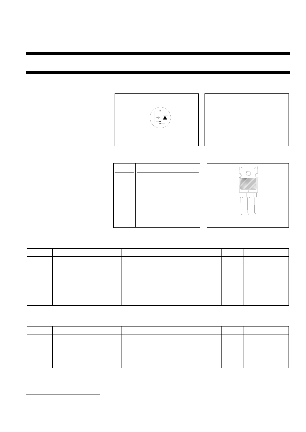
GENERAL DESCRIPTION PINNING SOT429 (TO247)
N-channel, enhancement mode PIN DESCRIPTION
field-effect power transistor,
intendedforuse in off-line switched 1 gate
mode power supplies, T.V. and
computer monitor power supplies, 2 drain
d.c.tod.c.converters,motorcontrol
circuits and general purpose 3 source
switching applications.
ThePHW14N50E is supplied in the
tab drain
2
1
3
SOT429 (TO247) conventional
leaded package.
LIMITING VALUES
Limiting values in accordance with the Absolute Maximum System (IEC 134)
SYMBOL PARAMETER CONDITIONS MIN. MAX. UNIT
V
DSS
V
DGR
V
GS
I
D
I
DM
P
D
Tj, T
Drain-source voltage Tj = 25 ˚C to 150˚C - 500 V
Drain-gate voltage Tj = 25 ˚C to 150˚C; RGS = 20 kΩ - 500 V
Gate-source voltage - ± 30 V
Continuous drain current Tmb = 25 ˚C; VGS = 10 V - 14 A
Tmb = 100 ˚C; VGS = 10 V - 9 A
Pulsed drain current Tmb = 25 ˚C - 56 A
Total dissipation Tmb = 25 ˚C - 192 W
Operating junction and - 55 150 ˚C
stg
storage temperature range
AVALANCHE ENERGY LIMITING VALUES
Limiting values in accordance with the Absolute Maximum System (IEC 134)
SYMBOL PARAMETER CONDITIONS MIN. MAX. UNIT
E
AS
E
AR
IAS, I
1 pulse width and repetition rate limited by Tj max.
January 1998 1 Rev 1.000
Non-repetitive avalanche Unclamped inductive load, ID = 14 A; - 910 mJ
energy VDD ≤ 50 V; starting Tj = 25˚C; RGS = 50 Ω;
VGS = 10 V
Repetitive avalanche energy
Repetitive and non-repetitive - 14 A
AR
1
-23mJ
avalanche current

Philips Semiconductors Preliminary specification
PowerMOS transistors PHW14N50E
Avalanche energy rated
THERMAL RESISTANCES
SYMBOL PARAMETER CONDITIONS MIN. TYP. MAX. UNIT
R
th j-mb
R
th j-a
ELECTRICAL CHARACTERISTICS
Tj = 25 ˚C unless otherwise specified
SYMBOL PARAMETER CONDITIONS MIN. TYP. MAX. UNIT
V
(BR)DSS
∆V
(BR)DSS
∆T
j
R
DS(ON)
V
GS(TO)
g
fs
I
DSS
I
GSS
Q
g(tot)
Q
gs
Q
gd
t
d(on)
t
r
t
d(off)
t
f
L
d
L
d
L
s
C
iss
C
oss
C
rss
Thermal resistance junction - - 0.65 K/W
to mounting base
Thermal resistance junction SOT78 package, in free air - 60 - K/W
to ambient SOT429 package, in free air - 45 - K/W
SOT404 package, pcb mounted, minimum - 50 - K/W
footprint
Drain-source breakdown VGS = 0 V; ID = 0.25 mA 500 - - V
voltage
/ Drain-source breakdown VDS = VGS; ID = 0.25 mA - 0.1 - %/K
voltage temperature
coefficient
Drain-source on resistance VGS = 10 V; ID = 7 A - 0.35 0.4 Ω
Gate threshold voltage VDS = VGS; ID = 0.25 mA 2.0 3.0 4.0 V
Forward transconductance VDS = 30 V; ID = 7 A 9 12 - S
Drain-source leakage current VDS = 500 V; VGS = 0 V - 1 20 µA
VDS = 400 V; VGS = 0 V; Tj = 125 ˚C - 50 500 µA
Gate-source leakage current VGS = ±30 V; VDS = 0 V - 10 200 nA
Total gate charge ID = 14 A; V
= 400 V; VGS = 10 V - 170 220 nC
DD
Gate-source charge - 5 15 nC
Gate-drain (Miller) charge - 95 130 nC
Turn-on delay time VDD = 250 V; RD = 18 Ω; - 35 - ns
Turn-on rise time RG = 4.7 Ω - 105 - ns
Turn-off delay time - 200 - ns
Turn-off fall time - 120 - ns
Internal drain inductance Measured from tab to centre of die - 3.5 - nH
Internal drain inductance Measured from drain lead to centre of die - 4.5 - nH
Internal source inductance Measured from source lead to source - 7.5 - nH
bond pad
Input capacitance VGS = 0 V; VDS = 25 V; f = 1 MHz - 2000 - pF
Output capacitance - 325 - pF
Feedback capacitance - 180 - pF
SOURCE-DRAIN DIODE RATINGS AND CHARACTERISTICS
Tj = 25 ˚C unless otherwise specified
SYMBOL PARAMETER CONDITIONS MIN. TYP. MAX. UNIT
I
S
I
SM
V
SD
t
rr
Q
rr
January 1998 2 Rev 1.000
Continuous source current Tmb = 25˚C - - 14 A
(body diode)
Pulsed source current (body Tmb = 25˚C - - 56 A
diode)
Diode forward voltage IS = 14 A; VGS = 0 V - - 1.5 V
Reverse recovery time IS = 14 A; VGS = 0 V; dI/dt = 100 A/µs - 600 - ns
Reverse recovery charge - 10 - µC
 Loading...