

Philips PHT6N03LT Datasheet
Philips Semiconductors Product specification
TrenchMOS transistor PHT6N03LT
Logic level FET
FEATURES SYMBOL QUICK REFERENCE DATA
• ’Trench’ technology V
d
• Very low on-state resistance
• Fast switching I
• Stable off-state characteristics
• High thermal cycling performance R
• Surface mounting package
g
R
s
≤ 30 mΩ (VGS = 5 V)
DS(ON)
≤ 28 mΩ (VGS = 10 V)
DS(ON)
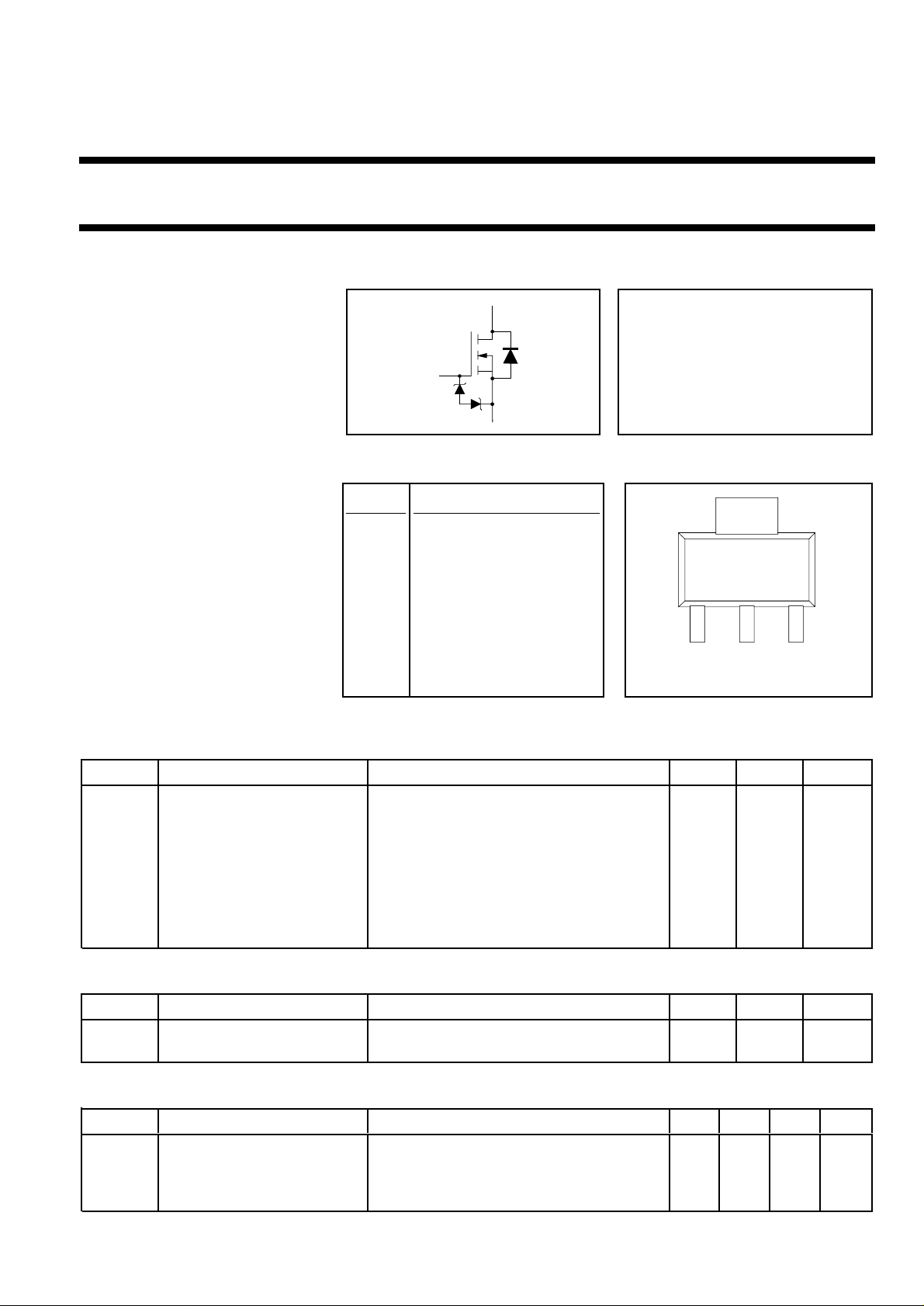
GENERAL DESCRIPTION PINNING SOT223
N-channel enhancement mode PIN DESCRIPTION
logic level field-effect power
transistor using ’trench’ 1 gate
technology. The device has very
low on-state resistance. It is 2 drain
intended for use in dc to dc
converters and general purpose 3 source
switching applications.
tab drain
The PHT6N03LT is supplied in the
SOT223 surface mounting
package.
LIMITING VALUES
Limiting values in accordance with the Absolute Maximum System (IEC 134)
= 30 V
DSS
= 5.9 A
D
1
4
23
SYMBOL PARAMETER CONDITIONS MIN. MAX. UNIT
V
DSS
V
DGR
V
GS
I
D
I
DM
P
D
Tj, T
Drain-source voltage Tj = 25 ˚C to 150˚C - 30 V
Drain-gate voltage Tj = 25 ˚C to 150˚C; RGS = 20 kΩ -30V
Gate-source voltage - ± 13 V
Continuous drain current T
= 25 ˚C; VGS = 10 V - 5.9 A
amb
T
= 100 ˚C; VGS = 10 V - 4.1 A
amb
Pulsed drain current - 23.6 A
Total power dissipation T
Operating junction and - 55 150 ˚C
stg
= 25 ˚C - 1.8 W
amb
storage temperature
ESD LIMITING VALUE
SYMBOL PARAMETER CONDITIONS MIN. MAX. UNIT
V
C
Electrostatic discharge Human body model (100 pF, 1.5 kΩ)-2kV
capacitor voltage, all pins
THERMAL RESISTANCES
SYMBOL PARAMETER CONDITIONS MIN. TYP. MAX. UNIT
R
R
th j-sp
th j-a
Thermal resistance junction mounted on any pcb - - 15 K/W
to solder point
Thermal resistance junction mounted on test pcb of fig:17 - 70 - K/W
to ambient
January 1998 1 Rev 1.300

Philips Semiconductors Product specification
TrenchMOS transistor PHT6N03LT
Logic level FET
ELECTRICAL CHARACTERISTICS
Tj= 25˚C unless otherwise specified
SYMBOL PARAMETER CONDITIONS MIN. TYP. MAX. UNIT
V
(BR)DSS
V
(BR)GSS
V
GS(TO)
R
DS(ON)
g
fs
I
DSS
I
GSS
Q
g(tot)
Q
gs
Q
gd
t
d on
t
r
t
d off
t
f
L
d
L
d
L
s
C
iss
C
oss
C
rss
Drain-source breakdown VGS = 0 V; ID = 0.25 mA; 30 - - V
voltage Tj = -55˚C 27 - - V
Gate-source breakdown IG = 1 mA 10 - - V
voltage
Gate threshold voltage VDS = VGS; ID = 1 mA 1 1.5 2 V
Tj = 150˚C 0.6 - - V
Tj = -55˚C - - 2.3 V
Drain-source on-state VGS = 5 V; ID = 3.2 A - 24 30 mΩ
resistance VGS = 10 V; ID = 3.2 A - 18 28 mΩ
VGS = 5 V; ID = 3.2 A; Tj = 150˚C - - 51 mΩ
Forward transconductance VDS = 25 V; ID = 5.9 A 8 14 - S
Zero gate voltage drain VDS = 30 V; VGS = 0 V; - 0.05 10 µA
current Tj = 150˚C - - 500 µA
Gate source leakage current VGS = ±5 V; VDS = 0 V - 0.02 1 µA
Tj = 150˚C - - 10 µA
Total gate charge ID = 5.9 A; V
= 24 V; VGS = 5 V - 24 - nC
DD
Gate-source charge - 3 - nC
Gate-drain (Miller) charge - 11 - nC
Turn-on delay time VDD = 15 V; ID = 5.9 A; - 30 45 ns
Turn-on rise time VGS = 5 V; RG = 5 Ω - 80 130 ns
Turn-off delay time Resistive load - 95 135 ns
Turn-off fall time - 40 55 ns
Internal drain inductance Measured from tab to centre of die - 3.5 - nH
Internal drain inductance Measured from drain lead to centre of die - 3.5 - nH
Internal source inductance Measured from source lead to source - 7.5 - nH
bond pad
Input capacitance VGS = 0 V; VDS = 25 V; f = 1 MHz - 1050 - pF
Output capacitance - 270 - pF
Feedback capacitance - 140 - pF
REVERSE DIODE LIMITING VALUES AND CHARACTERISTICS
Tj = 25˚C unless otherwise specified
SYMBOL PARAMETER CONDITIONS MIN. TYP. MAX. UNIT
I
S
I
SM
V
SD
t
rr
Q
rr
January 1998 2 Rev 1.300
Continuous source current - - 5.9 A
(body diode)
Pulsed source current (body - - 10 A
diode)
Diode forward voltage IF = 5.9 A; VGS = 0 V - 0.75 1.2 V
Reverse recovery time IF = 5.9 A; -dIF/dt = 100 A/µs; - 100 - ns
Reverse recovery charge VGS = -10 V; VR = 25 V - 0.4 - µC
 Loading...