

Philips pht1n60p DATASHEETS
Philips Semiconductors Objective specification
PowerMOS transistor PHT1N60R
GENERAL DESCRIPTION QUICK REFERENCE DATA
N-channel enhancement mode SYMBOL PARAMETER MAX. UNIT field-effect power transistor in a plastic envelope suitable for surface V mounting featuring high avalanche I energy capability, stable blocking P voltage, fast switching and high R thermal cycling performance.
DS
D
tot
DS(ON)
Intended for use in Compact Fluorescent Lights (CFL) and general
purpose switching applications.
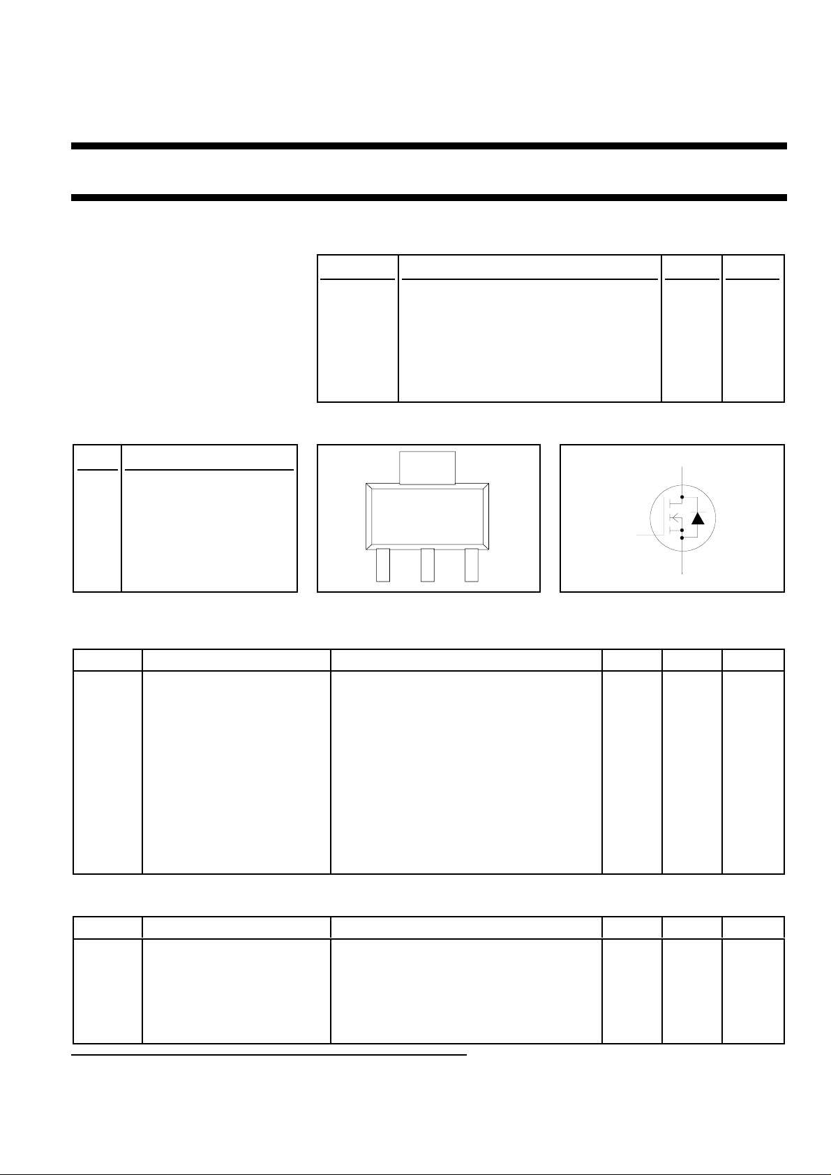
PINNING - SOT223 PIN CONFIGURATION SYMBOL
Drain-source voltage 600 V
Drain current (DC) 0.53 A
Total power dissipation 1.8 W
Drain-source on-state resistance 16.0 Ω
PIN DESCRIPTION
4
d
1 gate
2 drain
3 source
4 drain (tab)
1
23
g
s
LIMITING VALUES
Limiting values in accordance with the Absolute Maximum System (IEC 134)
SYMBOL PARAMETER CONDITIONS MIN. MAX. UNIT
V
V
±V
I
D
I
DM
I
DR
I
DRM
P
T
T
DS
DGR
GS
tot
stg
j
Drain-source voltage - 600 V
Drain-gate voltage RGS = 20 kΩ - 600 V
Gate-source voltage - 30 V
Drain current (DC) Tsp = 25 ˚C - 0.53 A
Tsp = 100 ˚C - 0.4 A
Drain current (pulse peak Tsp = 25 ˚C - 2.12 A
value)
Source-drain diode current Tsp = 25 ˚C - 0.53 A
(DC)
Source-drain diode current Tsp = 25 ˚C - 2.12 A
(pulse peak value)
Total power dissipation Tsp = 25 ˚C - 1.8 W
Storage temperature -55 150 ˚C
Junction temperature - 150 ˚C
AVALANCHE LIMITING VALUE
SYMBOL PARAMETER CONDITIONS MIN. MAX. UNIT
W
DSS
W
DSR
1. Pulse width and frequency limited by T
February 1998 1 Rev 1.000
Drain-source non-repetitive ID = 2 A ; VDD ≤ 50 V ; VGS = 10 V ;
unclamped inductive turn-off RGS = 50 Ω
energy Tj = 25˚C prior to surge - 20 mJ
1
Drain-source repetitive ID = 2 A ; VDD ≤ 50 V ; VGS = 10 V ; - 3.6 mJ
Tj = 100˚C prior to surge - 8 mJ
unclamped inductive turn-off RGS = 50 Ω ; Tj ≤ 150 ˚C
energy
j(max)

Philips Semiconductors Objective specification
PowerMOS transistor PHT1N60R
THERMAL RESISTANCES
SYMBOL PARAMETER CONDITIONS MIN. TYP. MAX. UNIT
R
th j-sp
R
th j-a
STATIC CHARACTERISTICS
Tmb = 25 ˚C unless otherwise specified
SYMBOL PARAMETER CONDITIONS MIN. TYP. MAX. UNIT
V
(BR)DSS
V
GS(TO)
I
DSS
I
GSS
R
DS(ON)
V
SD
Thermal resistance junction to - - 15 K/W
solder point
Thermal resistance junction to pcb mounted; minimum footprint - 156 - K/W
ambient pcb mounted; pad area as in fig:2 - 70 - K/W
Drain-source breakdown volt- VGS = 0 V; ID = 0.25 mA 600 - - V
age
Gate threshold voltage VDS = VGS; ID = 0.25 mA 2.0 3.0 4.0 V
Drain-source leakage current VDS = 500 V; VGS = 0 V; Tj = 25 ˚C - 1 100 µA
VDS = 400 V; VGS = 0 V; Tj = 125 ˚C - 0.1 1.0 mA
Gate-source leakage current VGS = ±35 V; VDS = 0 V - 4 100 nA
Drain-source on-state resis- VGS = 10 V; ID = 1 A - - 16.0 Ω
tance
Source-drain diode forward IF = 2 A ;VGS = 0 V - 0.85 1.2 V
voltage
DYNAMIC CHARACTERISTICS
Tmb = 25 ˚C unless otherwise specified
SYMBOL PARAMETER CONDITIONS MIN. TYP. MAX. UNIT
g
C
C
C
Q
Q
Q
t
t
t
t
t
Q
fs
iss
oss
rss
g(tot)
gs
gd
d on
r
d off
f
rr
rr
Forward transconductance VDS = 15 V; ID = 1 A 0.5 0.8 - S
Input capacitance VGS = 0 V; VDS = 25 V; f = 1 MHz - 75 100 pF
Output capacitance - 10 15 pF
Feedback capacitance - 5 10 pF
Total gate charge VGS = 10 V; ID = 2 A; V
Gate to source charge - .5 - nC
= 400 V - 5 - nC
DS
Gate to drain (Miller) charge - 3 - nC
Turn-on delay time VDD = 30 V; ID = 2 A; - 5 10 ns
Turn-on rise time VGS = 10 V; RGS = 50 Ω; - 15 20 ns
Turn-off delay time R
Turn-off fall time - 7 15 ns
= 50 Ω - 1520ns
GEN
Source-drain diode Reverse IF = 2 A; -dIF/dt = 100 A/µs; - 150 - ns
recovery time
Source-drain diode Reverse VGS = 0 V; VR = 100 V - 1.5 - µC
recovery charge
February 1998 2 Rev 1.000
 Loading...