

Philips PHP65N06LT Datasheet
Philips Semiconductors Product specification
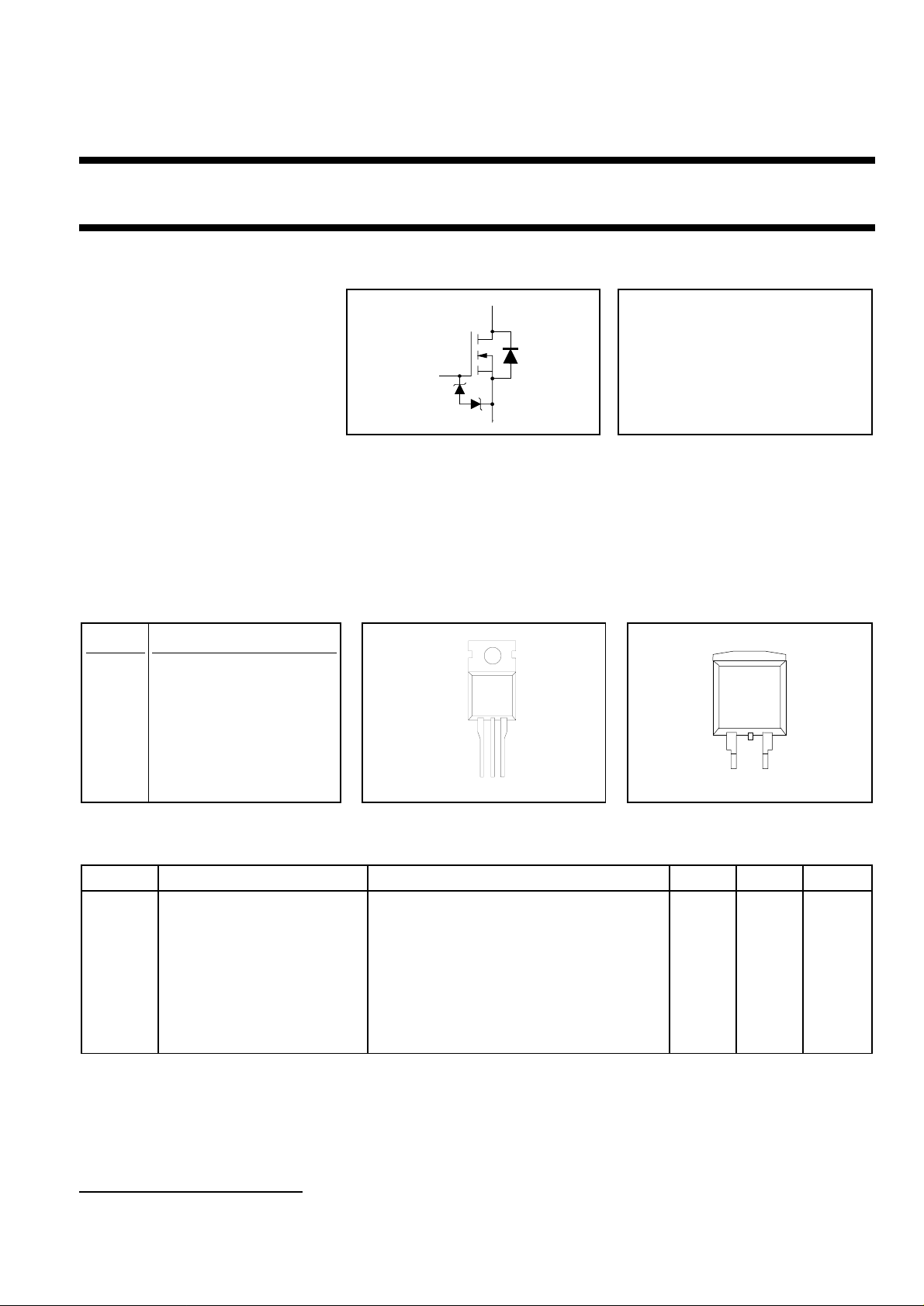
TrenchMOS transistor PHP65N06LT, PHB65N06LT
Logic level FET
FEATURES SYMBOL QUICK REFERENCE DATA
• ’Trench’ technology V
d
= 55 V
DSS
• Very low on-state resistance
• Fast switching I
= 63 A
D
• Stable off-state characteristics
• High thermal cycling performance R
• Low thermal resistance
g
R
s
≤ 18 mΩ (VGS = 5 V)
DS(ON)
≤ 16 mΩ (VGS = 10 V)
DS(ON)
GENERAL DESCRIPTION
N-channelenhancementmode,logic level, field-effect power transistor in a plastic envelopeusing’trench’technology.
Thedevicehas very low on-stateresistance. It is intended foruse in dc to dc converters and general purpose switching
applications.
The PHP65N06LT is supplied in the SOT78 (TO220AB) conventional leaded package.
The PHB65N06LT is supplied in the SOT404 surface mounting package.
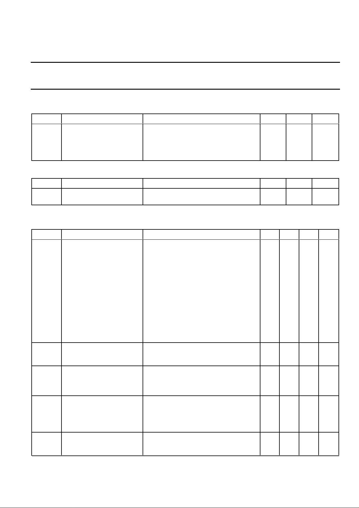
PINNING SOT78 (TO220AB) SOT404
PIN DESCRIPTION
1 gate
2 drain
1
3 source
tab drain
tab
123
tab
2
13
LIMITING VALUES
Limiting values in accordance with the Absolute Maximum System (IEC 134)
SYMBOL PARAMETER CONDITIONS MIN. MAX. UNIT
V
DSS
V
DGR
V
GS
I
D
I
DM
P
D
Tj, T
1 It is not possible to make connection to pin 2 of the SOT404 package.
January 1998 1 Rev 1.300
Drain-source voltage Tj = 25 ˚C to 175˚C - 55 V
Drain-gate voltage Tj = 25 ˚C to 175˚C; RGS = 20 kΩ -55V
Gate-source voltage - ± 13 V
Continuous drain current Tmb = 25 ˚C - 63 A
Tmb = 100 ˚C - 44 A
Pulsed drain current Tmb = 25 ˚C - 240 A
Total power dissipation Tmb = 25 ˚C - 150 W
Operating junction and - 55 175 ˚C
stg
storage temperature
Philips Semiconductors Product specification
TrenchMOS transistor PHP65N06LT, PHB65N06LT
Logic level FET
THERMAL RESISTANCES
SYMBOL PARAMETER CONDITIONS TYP. MAX. UNIT
R
th j-mb
R
th j-a
ESD LIMITING VALUE
SYMBOL PARAMETER CONDITIONS MIN. MAX. UNIT
V
C
ELECTRICAL CHARACTERISTICS
Tj= 25˚C unless otherwise specified
Thermal resistance junction - 1.0 K/W
to mounting base
Thermal resistance junction SOT78 package, in free air 60 - K/W
to ambient SOT404 package, pcb mounted, minimum 50 - K/W
footprint
Electrostatic discharge Human body model (100 pF, 1.5 kΩ)-2kV
capacitor voltage, all pins
SYMBOL PARAMETER CONDITIONS MIN. TYP. MAX. UNIT
V
(BR)DSS
Drain-source breakdown VGS = 0 V; ID = 0.25 mA; 55 - - V
voltage Tj = -55˚C 50 - - V
V
(BR)GSS
Gate-source breakdown IG = ±1 mA; 10 - - V
voltage
V
GS(TO)
Gate threshold voltage VDS = VGS; ID = 1 mA 1.0 1.5 2.0 V
Tj = 175˚C 0.5 - - V
Tj = -55˚C - - 2.3 V
R
DS(ON)
Drain-source on-state VGS = 5 V; ID = 25 A - 15 18 mΩ
resistance VGS = 10 V; ID = 25 A - 13 16 mΩ
Tj = 175˚C - - 38 mΩ
g
I
fs
GSS
Forward transconductance VDS = 25 V; ID = 25 A 25 52 - S
Gate source leakage current VGS = ±5 V; VDS = 0 V - 0.02 1 µA
Tj = 175˚C - - 20 µA
I
DSS
Zero gate voltage drain VDS = 55 V; VGS = 0 V; - 0.05 10 µA
current Tj = 175˚C - - 500 µA
Q
Q
Q
t
t
t
t
L
L
g(tot)
gs
gd
d on
r
d off
f
d
d
Total gate charge ID = 50 A; V
= 44 V; VGS = 5 V - 34 - nC
DD
Gate-source charge - 8 - nC
Gate-drain (Miller) charge - 17 - nC
Turn-on delay time VDD = 30 V; ID = 25 A; - 30 45 ns
Turn-on rise time VGS = 5 V; RG = 10 Ω - 80 130 ns
Turn-off delay time Resistive load - 100 140 ns
Turn-off fall time - 50 75 ns
Internal drain inductance Measured from tab to centre of die - 3.5 - nH
Internal drain inductance Measured from drain lead to centre of die - 4.5 - nH
(SOT78 package only)
L
s
Internal source inductance Measured from source lead to source - 7.5 - nH
bond pad
C
iss
C
oss
C
rss
Input capacitance VGS = 0 V; VDS = 25 V; f = 1 MHz - 2000 2600 pF
Output capacitance - 390 490 pF
Feedback capacitance - 200 290 pF
January 1998 2 Rev 1.300
Philips Semiconductors Product specification
TrenchMOS transistor PHP65N06LT, PHB65N06LT
Logic level FET
REVERSE DIODE LIMITING VALUES AND CHARACTERISTICS
Tj = 25˚C unless otherwise specified
SYMBOL PARAMETER CONDITIONS MIN. TYP. MAX. UNIT
I
S
I
SM
V
SD
t
rr
Q
rr
AVALANCHE LIMITING VALUE
SYMBOL PARAMETER CONDITIONS MIN. MAX. UNIT
W
DSS
Continuous source current - - 63 A
(body diode)
Pulsed source current (body - - 240 A
diode)
Diode forward voltage IF = 25 A; VGS = 0 V - 0.95 1.2 V
IF = 50 A; VGS = 0 V - 1.0 - V
Reverse recovery time IF = 50 A; -dIF/dt = 100 A/µs; - 48 - ns
Reverse recovery charge VGS = -10 V; VR = 30 V - 0.1 - µC
Drain-source non-repetitive ID = 50 A; VDD ≤ 25 V; VGS = 5 V; - 125 mJ
unclamped inductive turn-off RGS = 50 Ω; Tmb = 25 ˚C
energy
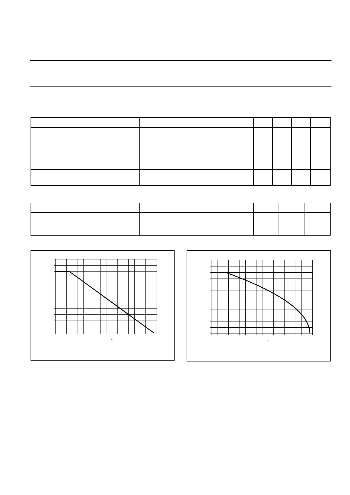
PD%
120
110
100
90
80
70
60
50
40
30
20
10
0
0 20 40 60 80 100 120 140 160 180
Normalised Power Derating
Tmb / C
Fig.1. Normalised power dissipation.
PD% = 100⋅PD/P
D 25 ˚C
= f(Tmb)
ID%
120
110
100
90
80
70
60
50
40
30
20
10
0
0 20 40 60 80 100 120 140 160 180
Normalised Current Derating
Tmb / C
Fig.2. Normalised continuous drain current.
ID% = 100⋅ID/I
= f(Tmb); conditions: VGS ≥ 5 V
D 25 ˚C
January 1998 3 Rev 1.300
 Loading...