

Philips PHP55N03T Datasheet
Philips Semiconductors Product specification
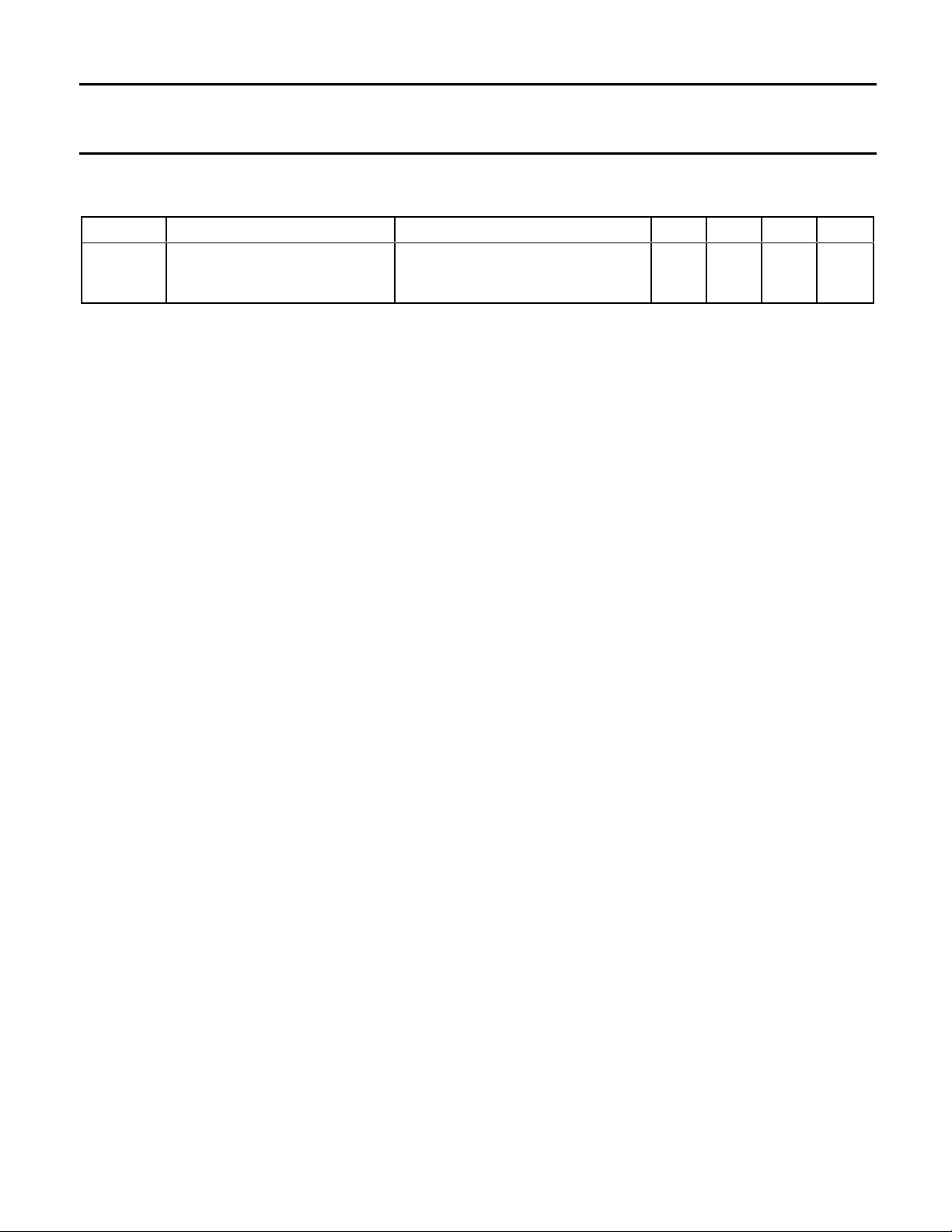
TrenchMOS transistor PHP55N03T
Standard level FET
GENERAL DESCRIPTION QUICK REFERENCE DATA
N-channel enhancement mode SYMBOL PARAMETER MAX. UNIT
standard level field-effect power
transistor in a plastic envelope using V
’trench’ technology. The device I
featuresverylowon-state resistance P
and has integral zener diodes giving T
ESD protection up to 2kV. It is R
DS
D
tot
j
DS(ON)
intended for use in DC-DC resistance VGS = 10 V
converters and general purpose
switching applications.
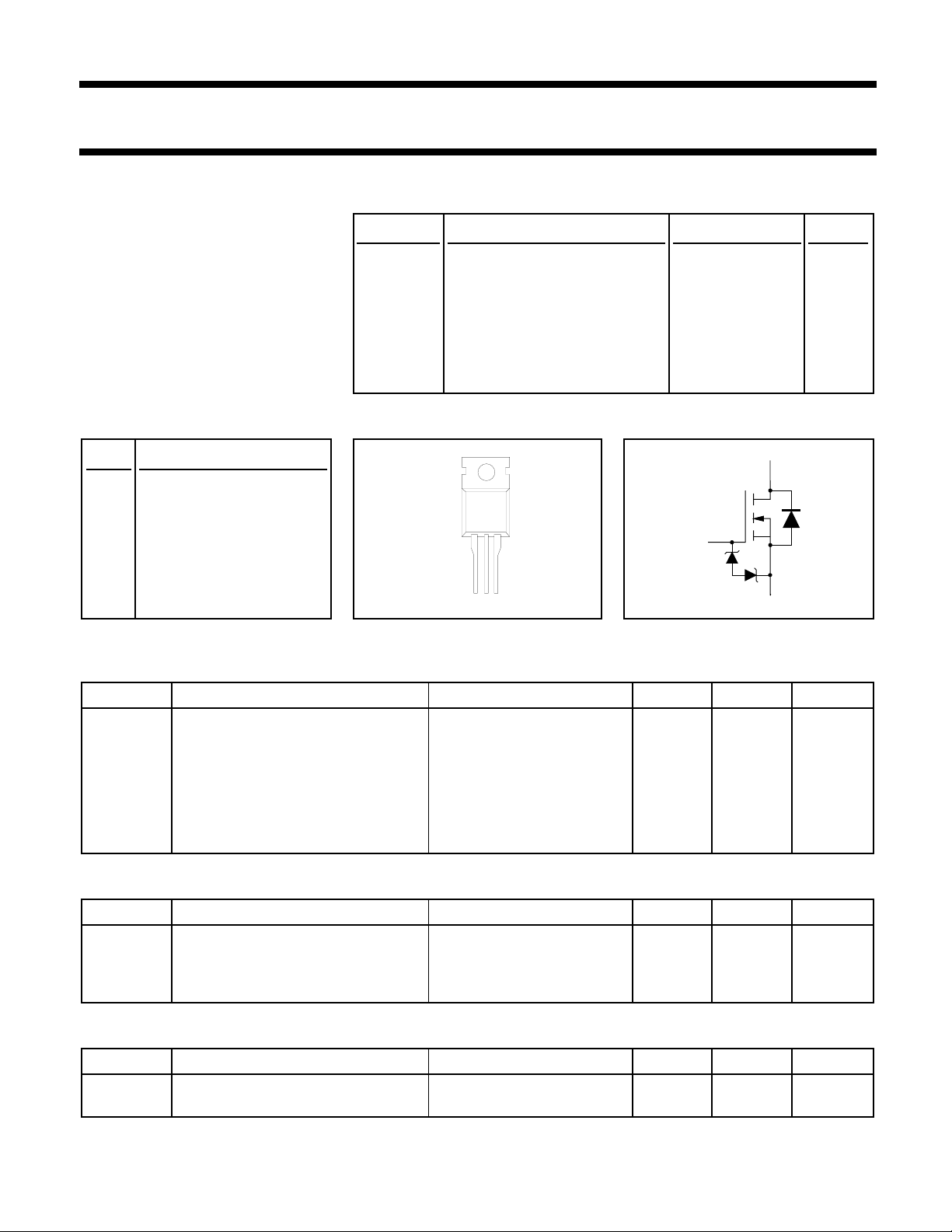
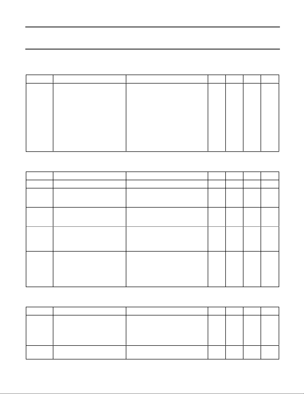
PINNING - TO220AB PIN CONFIGURATION SYMBOL
Drain-source voltage 30 V
Drain current (DC) 55 A
Total power dissipation 103 W
Junction temperature 175 ˚C
Drain-source on-state 18 mΩ
PIN DESCRIPTION
tab
d
1 gate
2 drain
3 source
tab drain
123
g
s
LIMITING VALUES
Limiting values in accordance with the Absolute Maximum System (IEC 134)
SYMBOL PARAMETER CONDITIONS MIN. MAX. UNIT
V
DS
V
DGR
Drain-source voltage - - 30 V
Drain-gate voltage RGS = 20 kΩ -30V
±VGSGate-source voltage - - 20 V
I
D
I
D
I
DM
P
tot
T
, T
stg
j
Drain current (DC) Tmb = 25 ˚C - 55 A
Drain current (DC) Tmb = 100 ˚C - 38 A
Drain current (pulse peak value) Tmb = 25 ˚C - 220 A
Total power dissipation Tmb = 25 ˚C - 103 W
Storage & operating temperature - - 55 175 ˚C
THERMAL RESISTANCES
SYMBOL PARAMETER CONDITIONS TYP. MAX. UNIT
R
th j-mb
Thermal resistance junction to - - 1.45 K/W
mounting base
R
th j-a
Thermal resistance junction to in free air 60 - K/W
ambient
ESD LIMITING VALUE
SYMBOL PARAMETER CONDITIONS MIN. MAX. UNIT
V
C
September 1997 1 Rev 1.100
Electrostatic discharge capacitor Human body model - 2 kV
voltage, all pins (100 pF, 1.5 kΩ)
Philips Semiconductors Product specification
TrenchMOS transistor PHP55N03T
Standard level FET
STATIC CHARACTERISTICS
Tj= 25˚C unless otherwise specified
SYMBOL PARAMETER CONDITIONS MIN. TYP. MAX. UNIT
V
(BR)DSS
V
GS(TO)
I
DSS
I
GSS
±V
(BR)GSS
R
DS(ON)
DYNAMIC CHARACTERISTICS
Tmb = 25˚C unless otherwise specified
Drain-source breakdown VGS = 0 V; ID = 0.25 mA; 30 - - V
voltage Tj = -55˚C 27 - - V
Gate threshold voltage VDS = VGS; ID = 1 mA 2.0 3.0 4.0 V
Tj = 175˚C 1.0 - - V
Tj = -55˚C - - 4.4
Zero gate voltage drain current VDS = 30 V; VGS = 0 V; - 0.05 10 µA
Tj = 175˚C - - 500 µA
Gate source leakage current VGS = ±10 V; VDS = 0 V - 0.02 1 µA
Tj = 175˚C - - 20 µA
Gate source breakdown voltage IG = ±1 mA; 16 - - V
Drain-source on-state VGS = 10 V; ID = 25 A - 15 18 mΩ
resistance Tj = 175˚C - - 33.5 mΩ
SYMBOL PARAMETER CONDITIONS MIN. TYP. MAX. UNIT
g
fs
Q
g(tot)
Q
gs
Q
gd
C
iss
C
oss
C
rss
t
d on
t
r
t
d off
t
f
L
d
Forward transconductance VDS = 25 V; ID = 25 A 7 15 - S
Total gate charge ID = 55 A; V
= 24 V; VGS = 10 V - 29.5 - nC
DD
Gate-source charge - 4.5 - nC
Gate-drain (Miller) charge - 16.5 - nC
Input capacitance VGS = 0 V; VDS = 25 V; f = 1 MHz - 1700 2000 pF
Output capacitance - 390 450 pF
Feedback capacitance - 170 220 pF
Turn-on delay time VDD = 15 V; ID = 25 A; - 15 20 ns
Turn-on rise time VGS = 10 V; RG = 5 Ω - 2235ns
Turn-off delay time Resistive load - 30 45 ns
Turn-off fall time - 18 25 ns
Internal drain inductance Measured from contact screw on - 3.5 - nH
tab to centre of die
L
d
Internal drain inductance Measured from drain lead 6 mm - 4.5 - nH
from package to centre of die
L
s
Internal source inductance Measured from source lead 6 mm - 7.5 - nH
from package to source bond pad
REVERSE DIODE LIMITING VALUES AND CHARACTERISTICS
Tj = 25˚C unless otherwise specified
SYMBOL PARAMETER CONDITIONS MIN. TYP. MAX. UNIT
I
DR
I
DRM
V
t
rr
Q
SD
rr
Continuous reverse drain - - 55 A
current
Pulsed reverse drain current - - 220 A
Diode forward voltage IF = 25 A; VGS = 0 V - 0.95 1.2 V
IF = 55 A; VGS = 0 V - 1.0 -
Reverse recovery time IF = 55 A; -dIF/dt = 100 A/µs; - 70 - ns
Reverse recovery charge VGS = -10 V; VR = 25 V - 0.1 - µC
September 1997 2 Rev 1.100
Philips Semiconductors Product specification
TrenchMOS transistor PHP55N03T
Standard level FET
AVALANCHE LIMITING VALUE
SYMBOL PARAMETER CONDITIONS MIN. TYP. MAX. UNIT
W
DSS
Drain-source non-repetitive ID = 28 A; VDD ≤ 25 V; - - 80 mJ
unclamped inductive turn-off VGS = 10 V; RGS = 50 Ω; Tmb = 25 ˚C
energy
September 1997 3 Rev 1.100
 Loading...