

Philips PHP4N50E Datasheet
Philips Semiconductors Objective specification
PowerMOS transistor PHP4N50E
GENERAL DESCRIPTION QUICK REFERENCE DATA
N-channel enhancement mode SYMBOL PARAMETER MAX. UNIT field-effect power transistor in a plastic envelope featuring high V avalanche energy capability, stable I blocking voltage, fast switching and P high thermal cycling performance R withlowthermalresistance.Intended
DS
D
tot
DS(ON)
for use in Switched Mode Power
Supplies (SMPS), motor control
circuits and general purpose
switching applications.
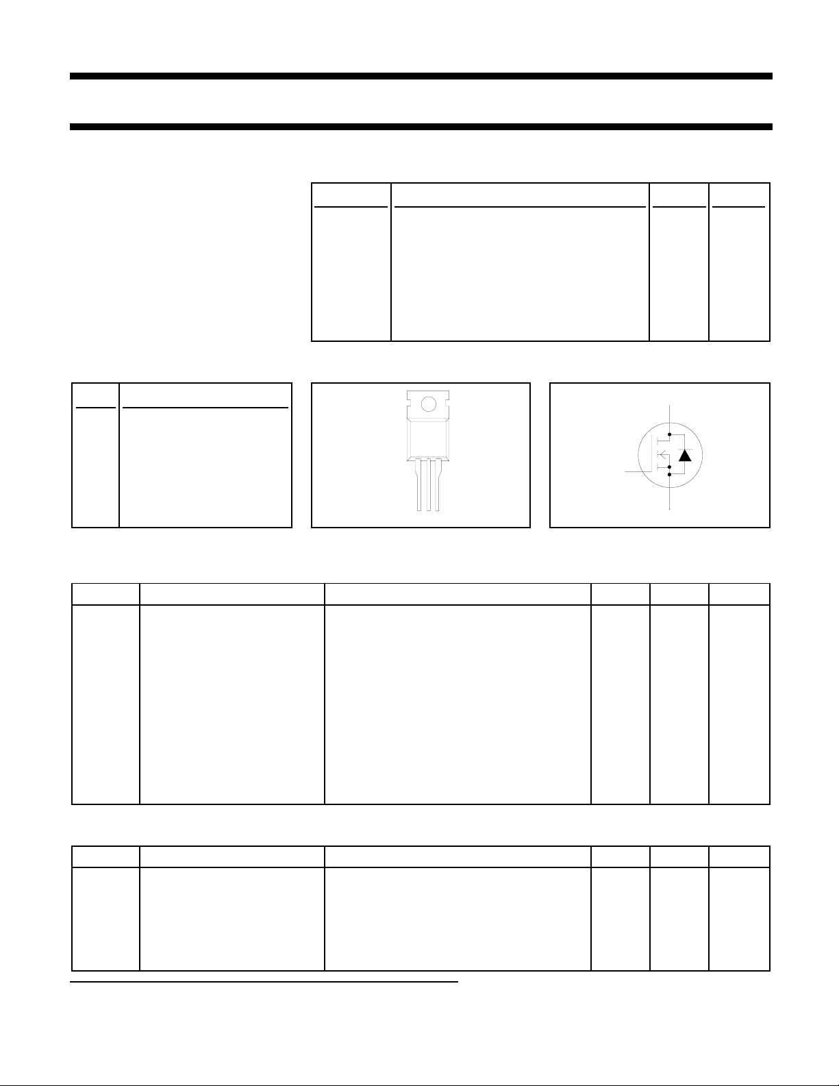
PINNING - TO220AB PIN CONFIGURATION SYMBOL
Drain-source voltage 500 V
Drain current (DC) 5.3 A
Total power dissipation 100 W
Drain-source on-state resistance 1.5 Ω
PIN DESCRIPTION
tab
d
1 gate
2 drain
3 source
tab drain
123
g
s
LIMITING VALUES
Limiting values in accordance with the Absolute Maximum System (IEC 134)
SYMBOL PARAMETER CONDITIONS MIN. MAX. UNIT
V
V
±V
I
D
I
DM
I
DR
I
DRM
P
T
T
DS
DGR
GS
tot
stg
j
Drain-source voltage - 500 V
Drain-gate voltage RGS = 20 kΩ - 500 V
Gate-source voltage - 30 V
Drain current (DC) Tmb = 25 ˚C - 5.3 A
Tmb = 100 ˚C - 3.3 A
Drain current (pulse peak Tmb = 25 ˚C - 21 A
value)
Source-drain diode current Tmb = 25 ˚C - 5.3 A
(DC)
Source-drain diode current Tmb = 25 ˚C - 21 A
(pulse peak value)
Total power dissipation Tmb = 25 ˚C - 100 W
Storage temperature -55 150 ˚C
Junction temperature - 150 ˚C
AVALANCHE LIMITING VALUE
SYMBOL PARAMETER CONDITIONS MIN. MAX. UNIT
W
DSS
W
DSR
Pulse width and frequency limited by T
October 1996 1 Rev 1.000
Drain-source non-repetitive ID = 5.3 A; VDD ≤ 50 V; VGS = 10 V;
unclamped inductive turn-off RGS = 50 Ω
energy Tj = 25˚C prior to surge - 280 mJ
1
Drain-source repetitive ID = 5.3 A; VDD ≤ 50 V; VGS = 10 V; - 7.4 mJ
Tj = 100˚C prior to surge - 44 mJ
unclamped inductive turn-off RGS = 50 Ω; Tj ≤ 150 ˚C
energy
j(max)
Philips Semiconductors Objective specification
PowerMOS transistor PHP4N50E
THERMAL RESISTANCES
SYMBOL PARAMETER CONDITIONS MIN. TYP. MAX. UNIT
R
th j-mb
R
th j-a
STATIC CHARACTERISTICS
Tmb = 25 ˚C unless otherwise specified
SYMBOL PARAMETER CONDITIONS MIN. TYP. MAX. UNIT
V
(BR)DSS
V
GS(TO)
I
DSS
I
GSS
R
DS(ON)
V
SD
Thermal resistance junction to - - 1.25 K/W
mounting base
Thermal resistance junction to - 60 - K/W
ambient
Drain-source breakdown VGS = 0 V; ID = 0.25 mA 500 - - V
voltage
Gate threshold voltage VDS = VGS; ID = 0.25 mA 2.0 3.0 4.0 V
Drain-source leakage current VDS = 500 V; VGS = 0 V; Tj = 25 ˚C - 10 100 µA
VDS = 400 V; VGS = 0 V; Tj = 125 ˚C - 0.1 1.0 mA
Gate-source leakage current VGS = ±30 V; VDS = 0 V - 10 100 nA
Drain-source on-state VGS = 10 V; ID = 2.65 A - 1.3 1.5 Ω
resistance
Source-drain diode forward IF = 5.3 A ;VGS = 0 V - 1.1 1.4 V
voltage
DYNAMIC CHARACTERISTICS
Tmb = 25 ˚C unless otherwise specified
SYMBOL PARAMETER CONDITIONS MIN. TYP. MAX. UNIT
g
C
C
C
Q
Q
Q
t
t
t
t
t
Q
L
L
L
fs
iss
oss
rss
g(tot)
gs
gd
d on
r
d off
f
rr
rr
d
d
s
Forward transconductance VDS = 15 V; ID = 2.65 A 1.5 2.5 - S
Input capacitance VGS = 0 V; VDS = 25 V; f = 1 MHz - 750 1000 pF
Output capacitance - 90 140 pF
Feedback capacitance - 40 70 pF
Total gate charge VGS = 10 V; ID = 5.3 A; V
Gate to source charge - 4 - nC
= 400 V - 35 - nC
DS
Gate to drain (Miller) charge - 16 - nC
Turn-on delay time VDD = 30 V; ID = 2.6 A; - 10 45 ns
Turn-on rise time VGS = 10 V; RGS = 50 Ω; - 45 60 ns
Turn-off delay time R
Turn-off fall time - 40 65 ns
= 50 Ω - 100 140 ns
GEN
Source-drain diode reverse IF = 5.3 A; -dIF/dt = 100 A/µs; - 1200 - ns
recovery time
Source-drain diode reverse VGS = 0 V; VR = 100 V - 6 - µC
recovery charge
Internal drain inductance Measured from contact screw on - 3.5 - nH
tab to centre of die
Internal drain inductance Measured from drain lead 6 mm - 4.5 - nH
from package to centre of die
Internal source inductance Measured from source lead 6 mm - 7.5 - nH
from package to source bond pad
October 1996 2 Rev 1.000
 Loading...