

Philips PHN708 Datasheet

DISCRETE SEMICONDUCTORS
DATA SH EET
PHN708
7 N-channel 80 mΩ FET array
enhancement mode MOS
transistors
Product specification
Supersedes data of 1997 Jun 19
File under Discrete Semiconductors, SC13
1998 Mar 17
Philips Semiconductors Product specification
7 N-channel 80 mΩ FET array
enhancement mode MOS transistors
FEATURES
• High-speed switching
• No secondary breakdown
• Very low on-state resistance.
APPLICATIONS
• Driving high performance three phase brushless
DC motors.
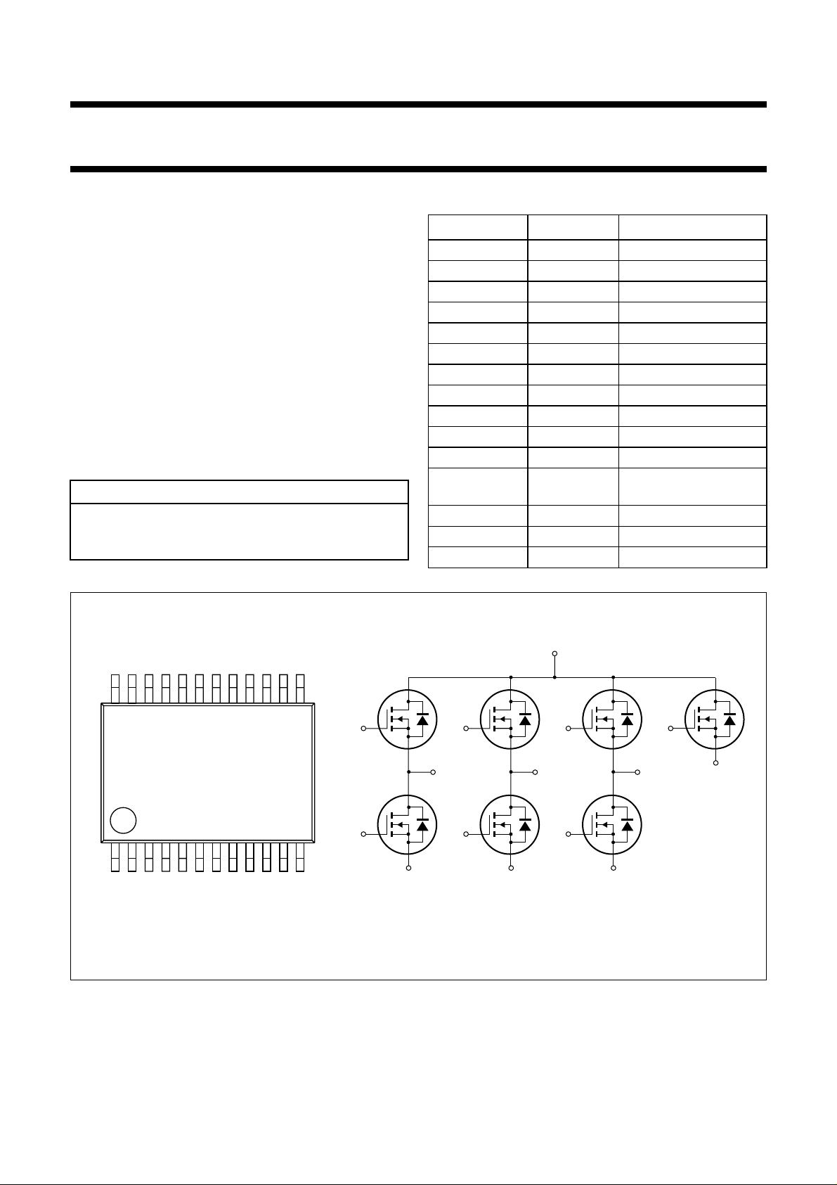
DESCRIPTION
Seven enhancement mode MOS transistors in a 24-pin
plastic SOT340-1 (SSOP24) package. Six of the
transistors are in three half-bridge configurations.
CAUTION
The device is supplied in an antistatic package.
The gate-source input must be protected against static
discharge during transport or handling.
PINNING - SOT340-1 (SSOP24)
PIN SYMBOL DESCRIPTION
1 and 4 d
2s
3g
5 and 8 d
6s
7g
9 and 12 d
10 s
11 g
13 g
14 s
15, 17, 18, 20,
d
1
1
1
2
2
2
3
3
3
4
4
4
drain 1
source 1
gate 1
drain 2
source 2
gate 2
drain 3
source 3
gate 3
gate 4
source 4
drain 4
21, 23, 24
16 g
19 g
22 g
5
6
7
gate 5
gate 6
gate 7
PHN708
handbook, full pagewidth
24 13
g
7
g
1
112
s
g
d
1
g
1
Fig.1 Simplified outline and symbol.
d
4
6
2
s
g
5
d
2
g
3
2
s
g
4
d
3
3
MAM275
s
4
1998 Mar 17 2
Philips Semiconductors Product specification
7 N-channel 80 mΩ FET array
PHN708
enhancement mode MOS transistors
QUICK REFERENCE DATA
SYMBOL PARAMETER CONDITIONS MIN. MAX. UNIT
V
DS
V
GS
V
GSth
I
D
R
DSon
P
tot
LIMITING VALUES
In accordance with the Absolute Maximum Rating System (IEC 134).
SYMBOL PARAMETER CONDITIONS MIN. MAX. UNIT
Per FET
V
DS
V
GS
I
D
I
DM
P
tot
T
stg
T
j
Source-drain diode
I
S
I
SM
drain-source voltage (DC) − 30 V
gate-source voltage (DC) −±20 V
gate-source threshold voltage ID= 1 mA; VDS=V
1 2.8 V
GS
drain current (DC) Ts=80°C − 3.1 A
drain-source on-state resistance ID= 1.5 A; VGS=10V − 80 mΩ
total power dissipation Ts=80°C − 1.3 W
drain-source voltage (DC) − 30 V
gate-source voltage (DC) −±20 V
drain current (DC) Ts=80°C; note 1 − 3.1 A
peak drain current note 2 − 12.4 A
total power dissipation Ts=80°C; note 3 − 1.3 W
T
=80°C; note 4 − 1.13 W
s
T
=80°C; note 5 − 0.92 W
s
T
=80°C; note 6 − 0.77 W
s
storage temperature −55 +150 °C
operating junction temperature −55 +150 °C
source current (DC) Ts=80°C − 1.3 A
peak source current note 2 − 5.2 A
Notes
1. T
is the temperature at the soldering point of the drain lead.
s
2. Pulse width and duty cycle limited by maximum junction temperature.
3. When only one FET dissipates.
4. When either combination of FETs 1-5, 1-6, 2-5, 2-7, 3-6 or 3-7 dissipate an equal amount of power.
5. When FET four plus either combination of FETs 1-5, 1-6, 2-5, 2-7, 3-6 or 3-7 dissipate an equal amount of power.
6. When all seven FETs dissipate an equal amount of power.
1998 Mar 17 3
Philips Semiconductors Product specification
7 N-channel 80 mΩ FET array
enhancement mode MOS transistors
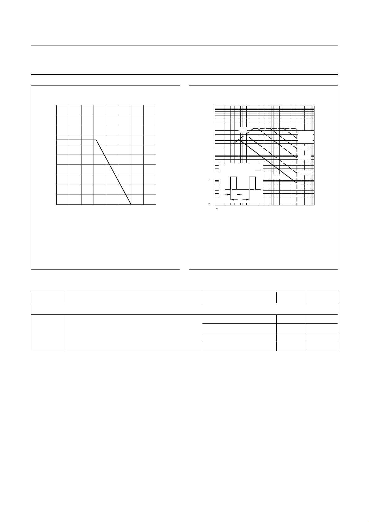
150
MDA787
Ts (°C)
200
handbook, halfpage
2
P
tot
(W)
1.6
1.2
0.8
0.4
0
0 50 100
2
10
handbook, halfpage
I
D
(A)
10
1
1
10
2
10
1
10
PHN708
MDA788
(1)
t
P
t
p
T
p
=
δ
T
DC
t
11010
tp =
100 µs
1 ms
10 ms
100 ms
VDS (V)
2
δ =0.01; Ts=80°C.
(1) R
Fig.2 Power derating curve.
DSon
limitation.
Fig.3 SOAR.
THERMAL CHARACTERISTICS
SYMBOL PARAMETER CONDITIONS VALUE UNIT
Per FET
R
th j-s
thermal resistance from junction to soldering point note 1 53 K/W
note 2 62 K/W
note 3 76 K/W
note 4 91 K/W
Notes
1. When only one FET dissipates.
2. When either combination of FETs 1-5, 1-6, 2-5, 2-7, 3-6 or 3-7 dissipate an equal amount of power.
3. When FET four plus either combination of FETs 1-5, 1-6, 2-5, 2-7, 3-6 or 3-7 dissipate an equal amount of power.
4. When all seven FETs dissipate an equal amount of power.
1998 Mar 17 4
 Loading...