

Philips PHKD3NQ10T Datasheet
Philips Semiconductors Product specification
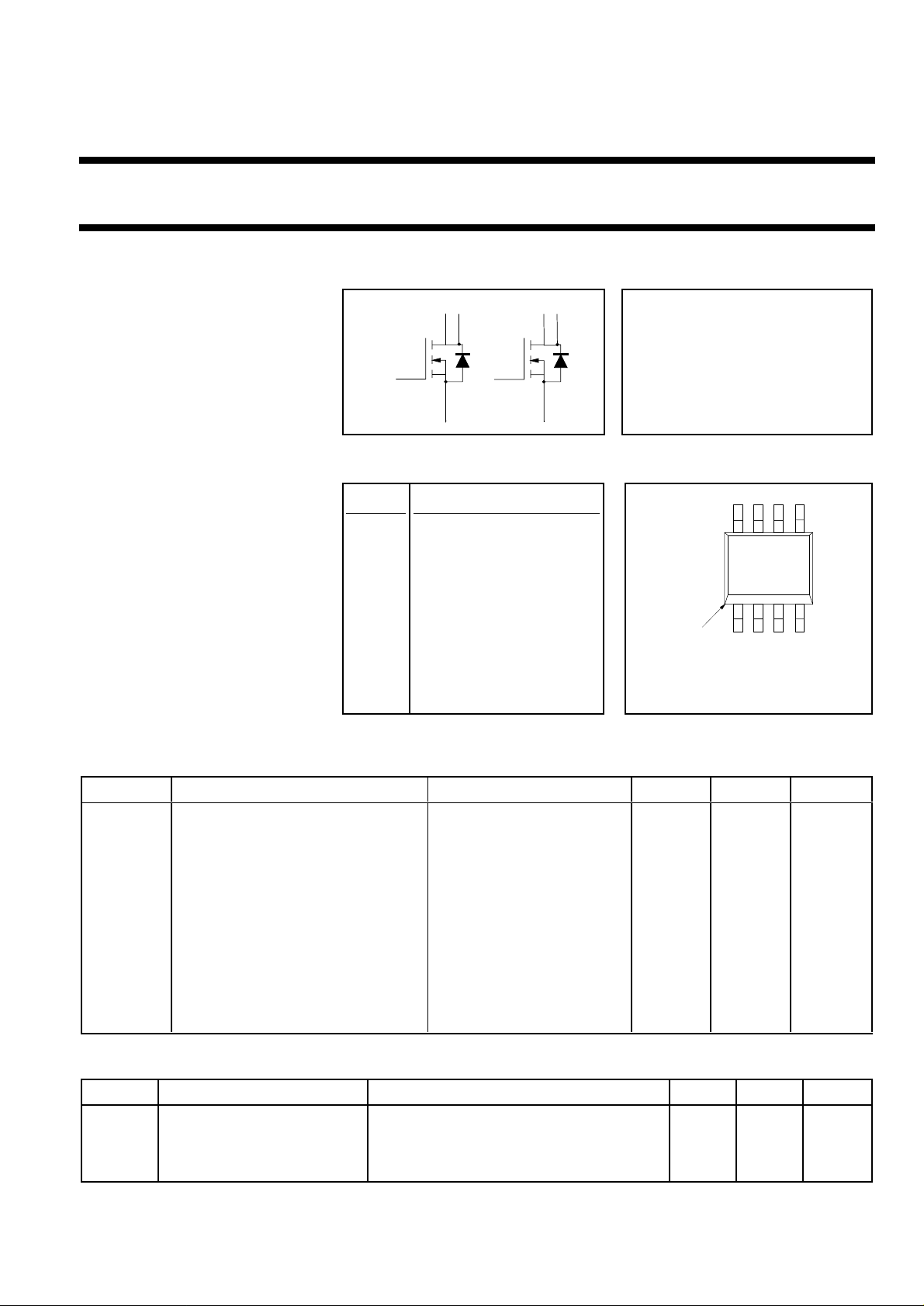
Dual N-channel TrenchMOSTM transistor PHKD3NQ10T
FEATURES SYMBOL QUICK REFERENCE DATA
• Dual device
d1
d2
• Low on-state resistance V
• Fast switching
• Low profile surface mount I
package
g1
s1
g2
s2
R
DS(ON)
≤ 90 mΩ (VGS = 10 V)
GENERAL DESCRIPTION PINNING SOT96-1
Dual N-channel enhancement PIN DESCRIPTION
mode field-effect transistor in a
plastic envelope using ’trench’ 1 source 1
technology.
2 gate 1
Applications:-
• Motor and relay drivers 3 source 2
• d.c. to d.c. converters
4 gate 2
pin 1 index
The PHKD3NQ10T is supplied in the SOT96-1 (SO8) surface 5,6 drain 2 mounting package.
7,8 drain 1
LIMITING VALUES
Limiting values in accordance with the Absolute Maximum System (IEC 134)
= 100 V
DS
= 3 A
D
1234
5678
SYMBOL PARAMETER CONDITIONS MIN. MAX. UNIT
V
DS
V
DGR
Continuous drain-source voltage Tj = 25 ˚C to 150˚C - 100 V
Drain-gate voltage Tj = 25 ˚C to 150˚C; - 100 V
RGS = 20 kΩ
V
GS
I
D
Gate-source voltage - ± 20 V
Drain current per MOSFET Ta = 25 ˚C, t ≤ 10 s - 3 A
Ta = 70 ˚C, t ≤ 10 s - 2.4 A
I
D
Drain current per MOSFET (both Ta = 25 ˚C, t ≤ 10 s - 2.2 A
MOSFETs conducting) Ta = 70 ˚C, t ≤ 10 s - 1.7 A
I
DM
Drain current (pulse peak value per Ta = 25 ˚C - 12 A
MOSFET)
P
tot
Total power dissipation Ta = 25 ˚C, t ≤ 10 s - 2 W
Ta = 70 ˚C, t ≤ 10 s - 1.3 W
T
stg
, T
j
Storage & operating temperature - 65 150 ˚C
THERMAL RESISTANCES
SYMBOL PARAMETER CONDITIONS TYP. MAX. UNIT
R
th j-a
R
th j-a
Thermal resistance junction Surface mounted on FR4 board, t ≤ 10 - 62.5 K/W
to ambient sec; either or both MOSFETs conducting
Thermal resistance junction Surface mounted on FR4 board; either or 150 - K/W
to ambient both MOSFETs conducting
August 1999 1 Rev 1.000

Philips Semiconductors Product specification
Dual N-channel TrenchMOSTM transistor PHKD3NQ10T
ELECTRICAL CHARACTERISTICS
Tj= 25˚C, per MOSFET unless otherwise specified
SYMBOL PARAMETER CONDITIONS MIN. TYP. MAX. UNIT
V
(BR)DSS
V
GS(TO)
R
DS(ON)
I
GSS
I
DSS
Q
g(tot)
Q
gs
Q
gd
t
d on
t
r
t
d off
t
f
L
d
L
s
C
iss
C
oss
C
rss
Drain-source breakdown VGS = 0 V; ID = 250 µA; 100 - - V
voltage Tj = -55˚C 89 - - V
Gate threshold voltage VDS = VGS; ID = 1 mA 2 3 4 V
Tj = 150˚C 1.1 - - V
Tj = -55˚C - 6 V
Drain-source on-state VGS = 10 V; ID = 1.5 A - 70 90 mΩ
resistance Tj = 150˚C - - 216 mΩ
Gate source leakage current VGS = ±20 V; VDS = 0 V - 10 100 nA
Zero gate voltage drain VDS = 100 V; VGS = 0 V; - 0.05 10 µA
current Tj = 150˚C - - 100 µA
Total gate charge ID = 3 A; V
= 80 V; VGS = 10 V - 21 - nC
DD
Gate-source charge - 2.5 - nC
Gate-drain (Miller) charge - 8 - nC
Turn-on delay time VDD = 50 V; RD = 15 Ω;-6-ns
Turn-on rise time VGS = 10 V; RG = 5.6 Ω -12-ns
Turn-off delay time Resistive load - 20 - ns
Turn-off fall time - 10 - ns
Internal drain inductance Measured from drain lead to centre of die - 2.5 - nH
Internal source inductance Measured from source lead to source - 5 - nH
bond pad
Input capacitance VGS = 0 V; VDS = 20 V; f = 1 MHz - 633 - pF
Output capacitance - 103 - pF
Feedback capacitance - 61 - pF
REVERSE DIODE LIMITING VALUES AND CHARACTERISTICS
Tj = 25˚C, per MOSFET unless otherwise specified
SYMBOL PARAMETER CONDITIONS MIN. TYP. MAX. UNIT
I
S
I
SM
V
SD
t
rr
Q
rr
Continuous source diode Ta = 25 ˚C, t ≤ 10 s - - 2 A
current
Pulsed source diode current - - 12 A
Diode forward voltage IF = 2 A; VGS = 0 V - 0.8 1.2 V
Reverse recovery time IF = 2 A; -dIF/dt = 100 A/µs; - 55 - ns
Reverse recovery charge VGS = 0 V; VR = 25 V - 135 - nC
August 1999 2 Rev 1.000
Philips Semiconductors Product specification
Dual N-channel TrenchMOSTM transistor PHKD3NQ10T
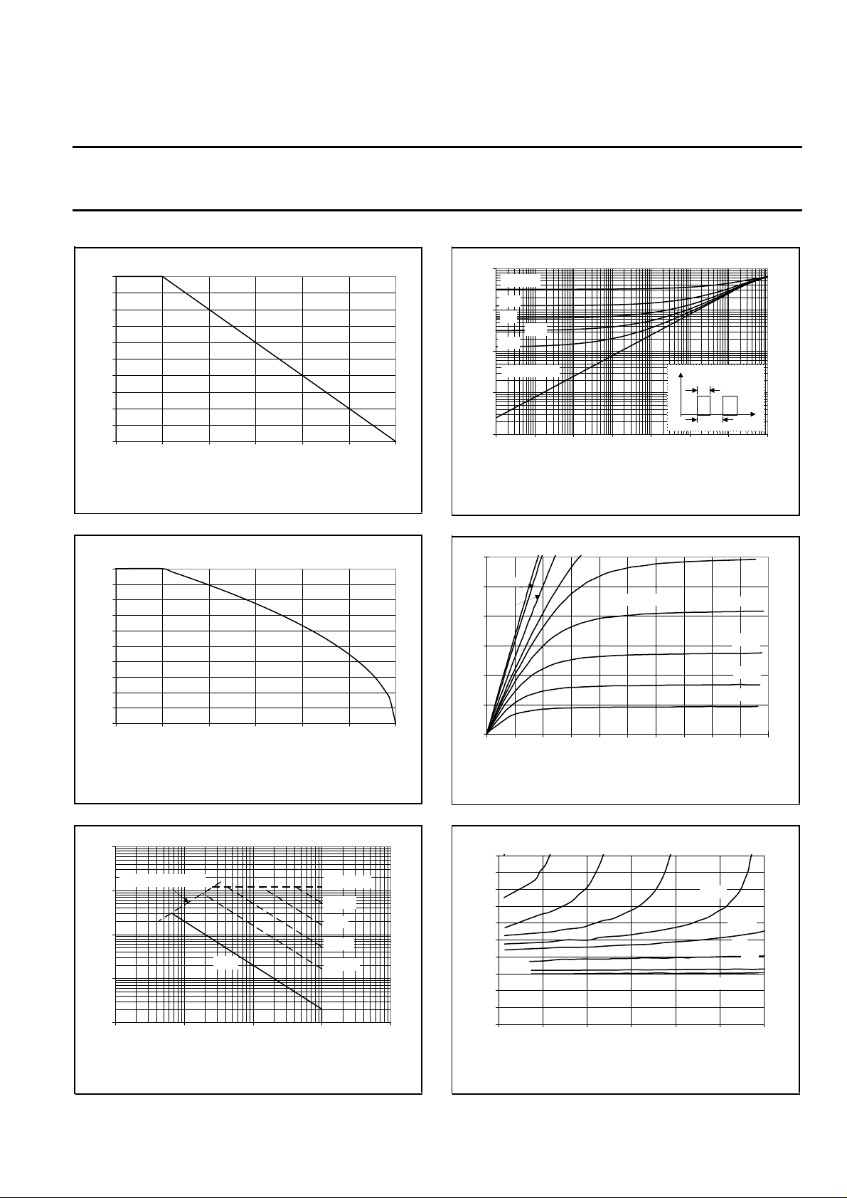
Normalised Power Derating, PD (%)
100
90
80
70
60
50
40
30
20
10
0
0 25 50 75 100 125 150
Ambient temperature, Ta (C)
Fig.1. Normalised power dissipation.
PD% = 100⋅PD/P
Normalised Current Derating, ID (%)
100
90
80
70
60
50
40
30
20
10
0
0 25 50 75 100 125 150
Ambient temperature, Ta (C)
D 25 ˚C
= f(Ta)
Fig.2. Normalised continuous drain current.
ID% = 100⋅ID/I
= f(Ta); VGS ≥ 10 V
D 25 ˚C
Transient thermal impedance, Zth j-a (K/W)
100
D = 0.5
0.2
10
0.1
0.05
0.02
1
single pulse
0.1
0.01
1E-06 1E-05 1E-04 1E-03 1E-02 1E-01 1E+00 1E+01
Pulse width, tp (s)
P
D
tp
D = tp/T
T
Fig.4. Transient thermal impedance.
Z
= f(t); parameter D = tp/T
th j-a
Drain Current, ID (A)
6
VGS = 10V
8 V
5
6 V
4
3
2
1
0
0 0.2 0.4 0.6 0.8 1 1.2 1.4 1.6 1.8 2
5.4 V
Tj = 25 C
Drain-Source Voltage, VDS (V)
5.2 V
5 V
4.8 V
4.6 V
4.4 V
Fig.5. Typical output characteristics, Tj = 25 ˚C
ID = f(VDS)
.
Peak Pulsed Drain Current, IDM (A)
100
RDS(on) = VDS/ ID
10
1
D.C.
0.1
0.01
0.1 1 10 100 1000
Drain-Source Voltage, VDS (V)
tp = 10 us
100 us
1 ms
10 ms
100 ms
Fig.3. Safe operating area
ID & IDM = f(VDS); IDM single pulse; parameter t
p
Drain-Source On Resistance, RDS(on) (Ohms)
0.2
4.6V
0.18
0.16
0.14
0.12
0.1
0.08
0.06
0.04
0.02
Tj = 25 C
0
0123456
4.8V
Drain Current, ID (A)
5 V
5.2 V
5.4 V
6V
8 V
VGS = 10V
Fig.6. Typical on-state resistance, Tj = 25 ˚C
R
= f(ID)
DS(ON)
.
August 1999 3 Rev 1.000
 Loading...