

Philips PHK12NQ10T User Manual

M3D315
1. Product profile
1.1 Description
1.2 Features
1.3 Applications
1.4 Quick reference data
PHK12NQ10T
TrenchMOS™ standard level FET
Rev. 01 — 15 September 2003 Product data
N-channel enhancement mode field-effect transistor in a plastic package using
TrenchMOS™ technology.
■ Surface mounting package ■ Low on-state resistance.
■ DC-to-DC converter primary side ■ Portable equipment applications.
■ VDS≤ 100 V ■ ID≤ 11.6 A
■ P
≤ 8.9 W ■ R
tot
DSon
2. Pinning information
Table 1: Pinning - SOT96-1 (SO8), simplified outline and symbol
Pin Description Simplified outline Symbol
1,2,3 source (s)
4 gate (g)
5,6,7,8 drain (d)
8
1
Top view MBK187
SOT96-1 (SO8)
5
4
≤ 28 mΩ
MBB076
d
g
s

Philips Semiconductors
PHK12NQ10T
TrenchMOS™ standard level FET
3. Ordering information
Table 2: Ordering information
Type number Package
Name Description Version
PHK12NQ10T SO8 Plastic small outline package; 8 leads. SOT96-1
4. Limiting values
Table 3: Limiting values
In accordance with the Absolute Maximum Rating System (IEC 60134).
Symbol Parameter Conditions Min Max Unit
V
DS
V
DGR
V
GS
I
D
I
DM
P
tot
T
stg
T
j
Source-drain diode
I
S
I
SM
Avalanche ruggedness
E
DS(AL)S
drain-source voltage (DC) 25 °C ≤ Tj≤ 150 °C - 100 V
drain-gate voltage (DC) 25 °C ≤ Tj≤ 150 °C; RGS=20kΩ - 100 V
gate-source voltage (DC) - ±20 V
drain current (DC) Tsp=25°C; VGS=10V;Figure 2 and 3 - 11.6 A
= 100 °C; VGS=10V;Figure 2 - 7.4 A
T
sp
peak drain current Tsp=25°C; pulsed; tp≤ 10 µs; Figure 3 -48A
total power dissipation Tsp=25°C; Figure 1 - 8.9 W
storage temperature −55 +150 °C
junction temperature −55 +150 °C
source (diode forward) current (DC) Tsp=25°C - 12 A
peak source (diode forward) current Tsp=25°C; pulsed; tp≤ 10 µs - 48 A
non-repetitive drain-source
avalanche energy
unclamped inductive load; ID= 11.5 A;
= 0.1 ms; VDD≤ 100 V; VGS=10V;
t
p
starting T
=25°C
j
-65mJ
9397 750 11949
Product data Rev. 01 — 15 September 2003 2 of 12
© Koninklijke Philips Electronics N.V. 2003. All rights reserved.
Philips Semiconductors
PHK12NQ10T
TrenchMOS™ standard level FET
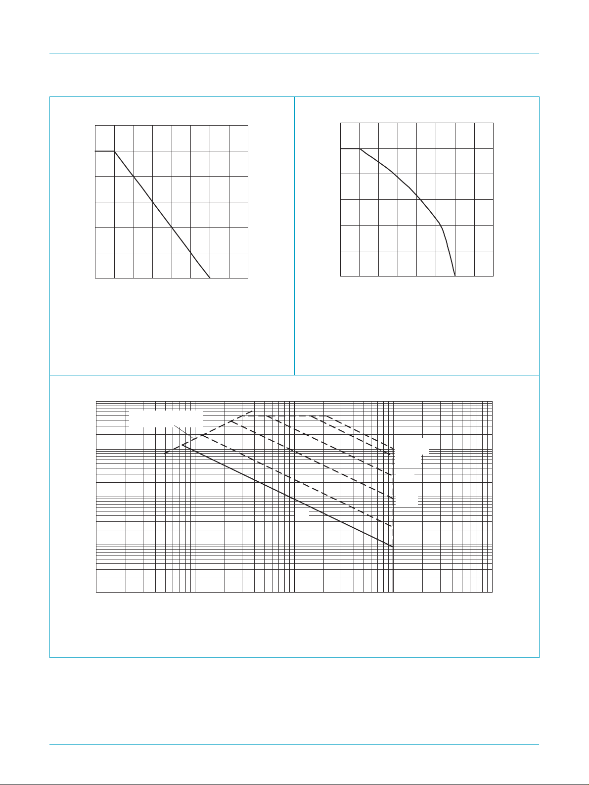
120
P
der
(%)
80
40
0
0 50 100 150 200
P
tot
P
der
-----------------------
P
tot 25 C°()
100%×= I
03aa17
Tsp (°C)
Fig 1. Normalized total power dissipation as a
function of solder point temperature.
2
10
I
D
(A)
10
Limit R
DSon
= V
DS
/ I
D
120
I
der
(%)
80
40
0
0 50 100 150 200
I
D
der
-------------------
I
D25C
()
100%×=
°
03aa25
Tsp (°C)
Fig 2. Normalized continuous drain current as a
function of solder point temperature.
003aaa509
tp = 10 µs
100 µs
1 ms
1
10
10
DC
-1
-2
-1
10
1 10 10
10 ms
100 ms
2
VDS (V)
10
3
Tsp=25°C; IDM is single pulse
Fig 3. Safe operating area; continuous and peak drain currents as a function of drain-source voltage.
9397 750 11949
Product data Rev. 01 — 15 September 2003 3 of 12
© Koninklijke Philips Electronics N.V. 2003. All rights reserved.
Philips Semiconductors
PHK12NQ10T
TrenchMOS™ standard level FET
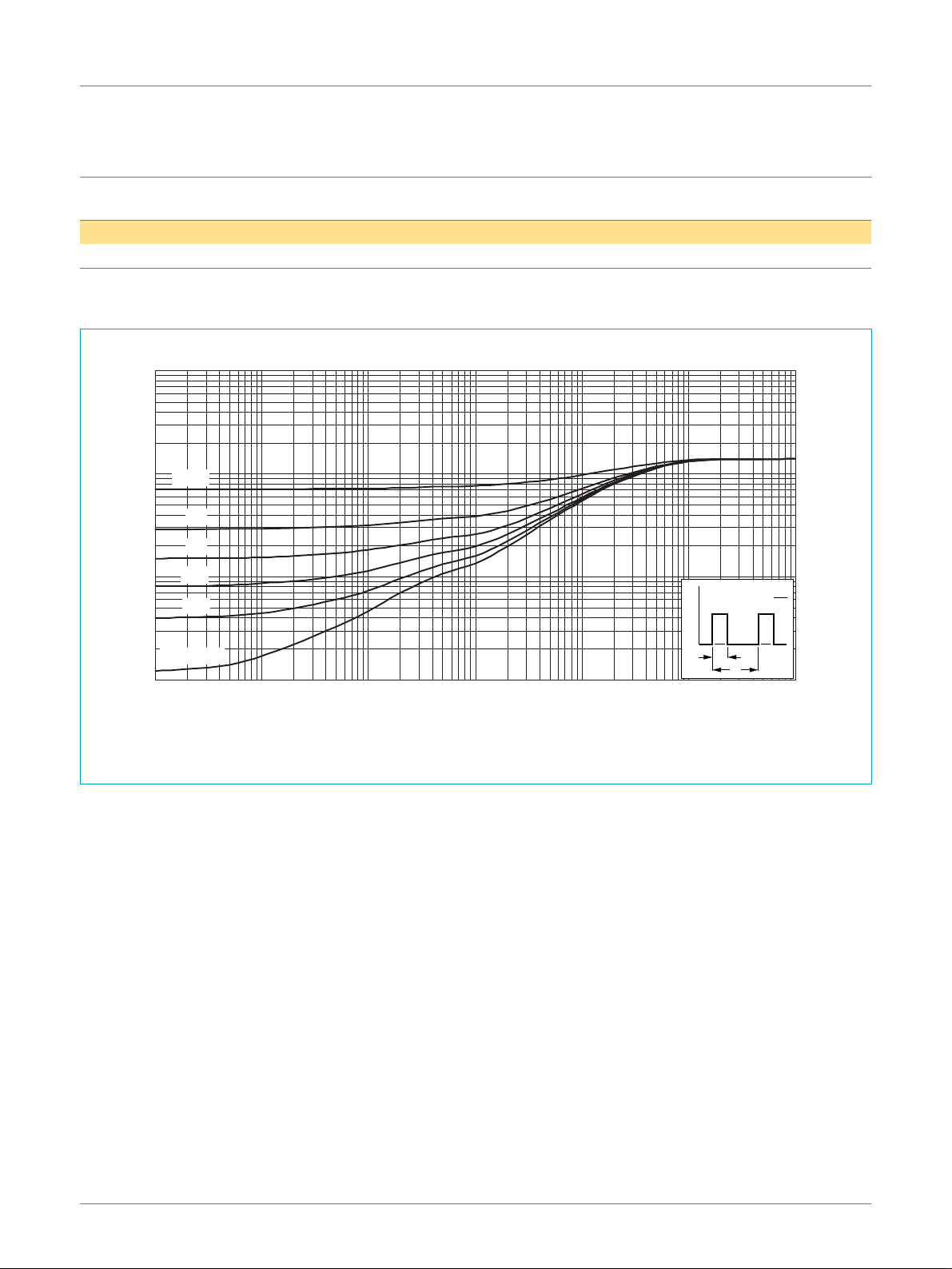
5. Thermal characteristics
Table 4: Thermal characteristics
Symbol Parameter Conditions Min Typ Max Unit
R
th(j-sp)
thermal resistance from junction to solder point Figure 4 --15K/W
5.1 Transient thermal impedance
2
10
Z
th(j-sp)
(K/W)
10
1
10
-1
single pulse
-5
10
δ =
0.5
0.2
0.1
0.05
0.02
P
t
p
T
-4
10
-3
10
-2
10
-1
10
1 10
tp (s)
Fig 4. Transient thermal impedance from junction to solder point as a function of pulse duration.
003aaa510
t
p
δ =
T
t
9397 750 11949
© Koninklijke Philips Electronics N.V. 2003. All rights reserved.
Product data Rev. 01 — 15 September 2003 4 of 12
 Loading...