

Philips PHC21025 Datasheet

DISCRETE SEMICONDUCTORS
DATA SH EET
PHC21025
Complementary enhancement
mode MOS transistors
Product specification
Supersedes data of November 1994
File under Discrete Semiconductors, SC13b
1997 Jun 20
Philips Semiconductors Product specification
Complementary enhancement
mode MOS transistors
FEATURES
• High-speed switching
• No secondary breakdown
• Very low on-resistance.
APPLICATIONS
• Motor and actuator driver
• Power management
• Synchronized rectification.
DESCRIPTION
One N-channel and one P-channel enhancement mode
MOS transistor in an 8-pin plastic SOT96-1 (SO8)
package.
CAUTION
The device is supplied in an antistatic package.
The gate-source input must be protected against static
discharge during transport or handling.
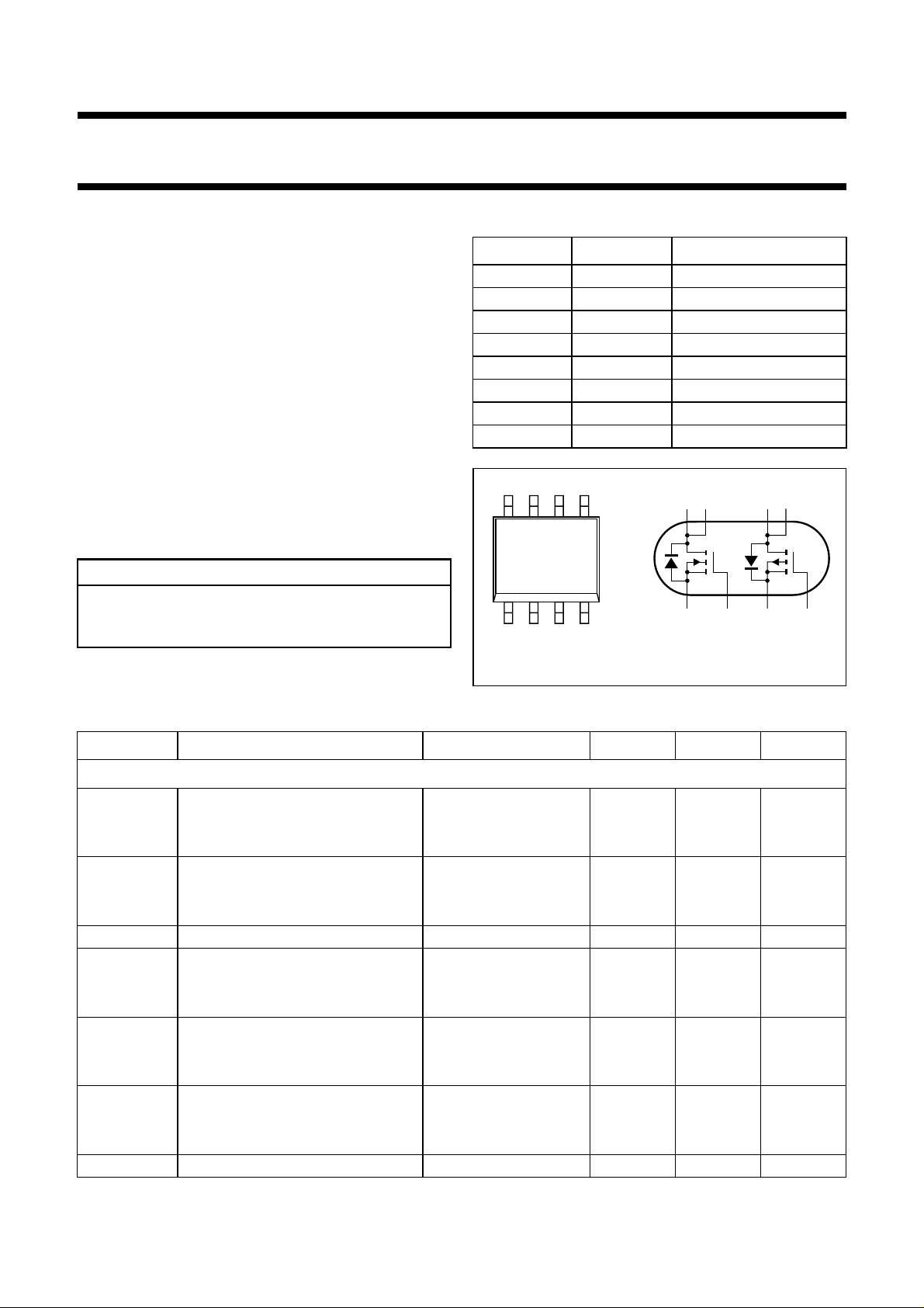
PINNING - SOT96-1 (SO8)
PIN SYMBOL DESCRIPTION
1s
2g
3s
4g
5d
6d
7d
8d
handbook, halfpage
58
1
4
MAM118
1
1
2
2
2
2
1
1
source 1
gate 1
source 2
gate 2
drain 2
drain 2
drain 1
drain 1
d
d
1
1
g
s
1
PHC21025
d
d
2
2
g
s
1
2
2
Fig.1 Simplified outline and symbol.
QUICK REFERENCE DATA
SYMBOL PARAMETER CONDITIONS MIN. MAX. UNIT
Per channel
V
DS
drain-source voltage (DC)
N-channel − 30 V
P-channel −−30 V
V
V
V
I
D
SD
GSO
GSth
source-drain diode forward voltage
N-channel I
P-channel I
= 1.25 A − 1.2 V
S
= −1.25 A −−1.6 V
S
gate-source voltage (DC) open drain −±20 V
gate-source threshold voltage V
N-channel V
P-channel V
DS=VGS;ID
DS=VGS
= 1 mA 1 2.8 V
; ID= −1mA −1 −2.8 V
drain current (DC)
N-channel − 3.5 A
P-channel −−2.3 A
R
P
DSon
tot
drain-source on-state resistance
N-channel V
P-channel V
=10V; ID= 2.2 A − 0.1 Ω
GS
= −10 V; ID= −1A − 0.25 Ω
GS
total power dissipation Ts=80°C − 2W
1997 Jun 20 2

Philips Semiconductors Product specification
Complementary enhancement
PHC21025
mode MOS transistors
LIMITING VALUES
In accordance with the Absolute Maximum Rating System (IEC 134).
SYMBOL PARAMETER CONDITIONS MIN. MAX. UNIT
Per channel
V
DS
V
GSO
I
D
I
DM
P
tot
T
stg
T
j
Source-drain diode
I
S
I
SM
drain-source voltage (DC)
N-channel − 30 V
P-channel −−30 V
gate-source voltage (DC) open drain −±20 V
drain current (DC) Ts≤ 80 °C
N-channel − 3.5 A
P-channel −−2.3 A
peak drain current note 1
N-channel − 14 A
P-channel −−10 A
total power dissipation Ts=80°C; note 2 − 2W
T
=25°C; note 3 − 2W
amb
T
=25°C; note 4 − 1W
amb
T
=25°C; note 5 − 1.3 W
amb
storage temperature −65 +150 °C
operating junction temperature − 150 °C
source current (DC) Ts≤ 80 °C
N-channel − 1.5 A
P-channel −−1.25 A
peak pulsed source current note 1
N-channel − 6A
P-channel −−5A
Notes
1. Pulse width and duty cycle limited by maximum junction temperature.
2. Maximum permissible dissipation per MOS transistor. Both devices may be loaded up to 2 W at the same time.
3. Maximum permissible dissipation per MOS transistor. Device mounted on printed-circuit board with an R
th a-tp
(ambient to tie-point) of 27.5 K/W.
4. Maximum permissible dissipation per MOS transistor. Device mounted on printed-circuit board with an R
th a-tp
(ambient to tie-point) of 90 K/W.
5. Maximum permissible dissipation if only one MOS transistor dissipates. Device mounted on printed-circuit board with
an R
(ambient to tie-point) of 90 K/W.
th a-tp
1997 Jun 20 3
Philips Semiconductors Product specification
Complementary enhancement
mode MOS transistors
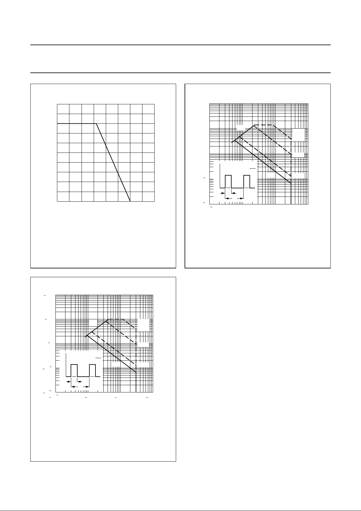
2.5
handbook, halfpage
P
tot
(W)
2.0
1.5
1.0
0.5
0
0 200
50 100 150
T ( C)
s
MLB836
o
2
10
handbook, halfpage
I
D
(A)
10
1
1
10
2
10
1
10
δ =0.01.
Ts=80°C.
(1) R
DSon
limitation.
PHC21025
MLB833 - 1
(1)
t
P
t
p
T
p
=
δ
T
DC
t
11010
tp =
10 µs
1 ms
0.1 s
(V)
2
V
DS
2
10
handbook, halfpage
I
D
(A)
10
1
1
10
2
10
1
10
δ = 0.01.
Ts=80°C.
(1) R
DSon
limitation.
Fig.2 Power derating curve.
(1)
t
P
t
p
T
p
=
δ
T
DC
t
11010
MBE155
tp =
10 µs
1 ms
0.1 s
V
(V)
DS
Fig.3 SOAR; N-channel.
2
Fig.4 SOAR; P-channel.
1997 Jun 20 4

Philips Semiconductors Product specification
Complementary enhancement
PHC21025
mode MOS transistors
THERMAL CHARACTERISTICS
SYMBOL PARAMETER VALUE UNIT
R
th j-s
CHARACTERISTICS
=25°C unless otherwise specified.
T
j
SYMBOL PARAMETER CONDITIONS MIN. TYP. MAX. UNIT
Per channel
V
(BR)DSS
V
GSth
I
DSS
I
GSS
I
Don
R
DSon
y
forward transfer admittance
fs
C
iss
C
oss
thermal resistance from junction to soldering point 35 K/W
drain-source breakdown voltage
N-channel V
P-channel V
= 0; ID=10µA30−−V
GS
= 0; ID= −10 µA −30 −−V
GS
gate-source threshold voltage
N-channel V
P-channel V
GS=VDS
GS=VDS
; ID= 1 mA 1 − 2.8 V
; ID= −1mA −1 −−2.8 V
drain-source leakage current
N-channel V
P-channel V
= 0; VDS=24V −−100 nA
GS
= 0; VDS= −24 V −−−100 nA
GS
gate leakage current VGS= ±20 V; VDS=0
N-channel −−±100 nA
P-channel −−±100 nA
on-state drain current
N-channel V
P-channel V
=10V; VDS= 1 V 3.5 −−A
GS
V
= 4.5 V; VDS=5V 2 −−A
GS
= −10 V; VDS=−1V −2.3 −−A
GS
V
= −4.5 V; VDS= −5V −1 −−A
GS
drain-source on-state resistance
N-channel V
P-channel V
N-channel V
P-channel V
= 4.5 V; ID=1A − 0.11 0.2 Ω
GS
V
=10V; ID= 2.2 A − 0.08 0.1 Ω
GS
= −4.5 V; ID= − 0.5 A − 0.33 0.4 Ω
GS
= −10 V; ID= −1A − 0.22 0.25 Ω
V
GS
=20V; ID= 2.2 A 2 4.5 − S
DS
= −20 V; ID= −1A 1 2 − S
DS
input capacitance
N-channel V
P-channel V
= 0; VDS= 20 V; f = 1 MHz − 250 − pF
GS
= 0; VDS= −20 V; f = 1 MHz − 250 − pF
GS
output capacitance
N-channel V
P-channel V
= 0; VDS= 20 V; f = 1 MHz − 140 − pF
GS
= 0; VDS= −20 V; f = 1 MHz − 140 − pF
GS
1997 Jun 20 5
 Loading...