

Philips PHC20306 Datasheet

DISCRETE SEMICONDUCTORS
DATA SH EET
PHC20306
Complementary enhancement
mode MOS transistor
Objective specification
File under Discrete Semiconductors, SC13b
1998 Feb 18
Philips Semiconductors Objective specification
Complementary enhancement
mode MOS transistor
FEATURES
• Very low on-state resistance
• High-speed switching
• No secondary breakdown.
APPLICATIONS
• Motor and actuator driver
• Power management
• Synchronized rectification.
DESCRIPTION
One N-channel and one P-channel enhancement mode
MOS transistor in an 8-pin SOT96-1 (SO8) plastic
package.
CAUTION
The device is supplied in an antistatic package.
The gate-source input must be protected against static
discharge during transport or handling.
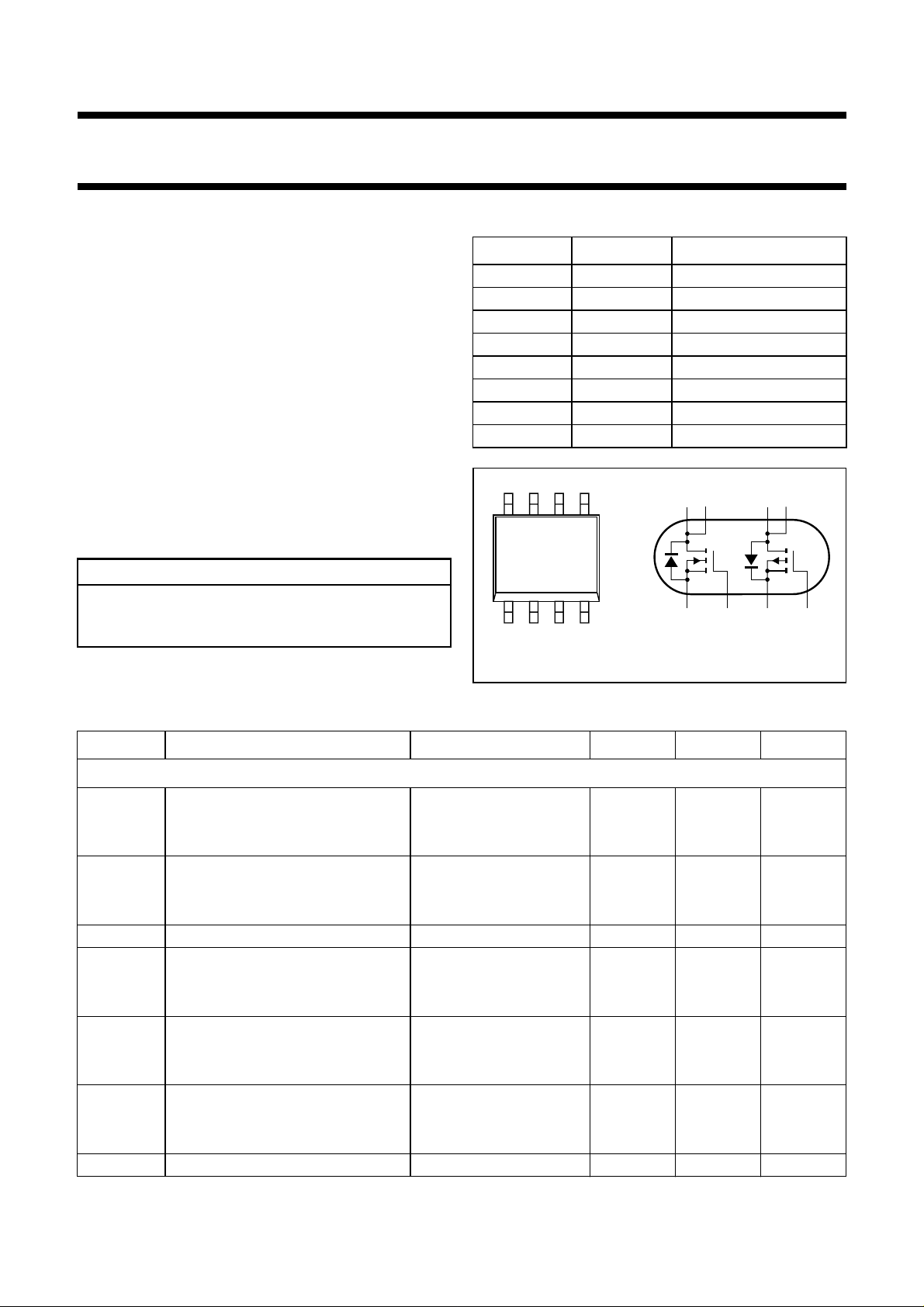
PINNING - SOT96-1 (SO8)
PIN SYMBOL DESCRIPTION
1s
2g
3s
4g
5d
6d
7d
8d
handbook, halfpage
1
58
4
MAM118
1
1
2
2
2
2
1
1
source 1
gate 1
source 2
gate 2
drain 2
drain 2
drain 1
drain 1
d1d
1
g
s
1
Fig.1 Simplified outline and symbol.
PHC20306
d2d
2
s
1
g
2
2
QUICK REFERENCE DATA
SYMBOL PARAMETER CONDITIONS MIN. MAX. UNIT
Per channel
V
DS
drain-source voltage (DC)
N-channel − 30 V
P-channel −−30 V
V
V
V
I
D
SD
GSO
GSth
source-drain diode forward voltage
N-channel V
P-channel V
= 0; IS= 1.25 A − 1V
GD
= 0; IS= −1.25 A −−1.3 V
GD
gate-source voltage (DC) open drain −±20 V
gate-source threshold voltage V
N-channel V
P-channel V
DS=VGS;ID
DS=VGS
= 1 mA 1 − V
; ID= −1mA −1 − V
drain current (DC) Ts=80°C
N-channel − 8.2 A
P-channel −−5.6 A
R
P
DSon
tot
drain-source on-state resistance
N-channel V
P-channel V
= 10 V; ID=4A − 30 mΩ
GS
= −10 V; ID= −2.8 A − 65 mΩ
GS
total power dissipation Ts=80°C − 3.5 W
1998 Feb 18 2

Philips Semiconductors Objective specification
Complementary enhancement
PHC20306
mode MOS transistor
LIMITING VALUES
In accordance with the Absolute Maximum Rating System (IEC 134).
SYMBOL PARAMETER CONDITIONS MIN. MAX. UNIT
Per channel
V
DS
V
GSO
I
D
I
DM
P
tot
T
stg
T
j
Source-drain diode
I
S
I
SM
drain-source voltage (DC)
N-channel − 30 V
P-channel −−30 V
gate-source voltage (DC) open drain −±20 V
drain current (DC) Ts=80°C; note 1
N-channel − 8.2 A
P-channel −−5.6 A
peak drain current note 2
N-channel − 33 A
P-channel −−22.5 A
total power dissipation Ts=80°C; note 3 − 3.5 W
T
=25°C; note 4 − 2.6 W
amb
T
=25°C; note 5 − 1.1 W
amb
T
=25°C; note 6 − 1.5 W
amb
storage temperature −55 +150 °C
operating junction temperature −55 +150 °C
source current (DC) Ts=80°C
N-channel − 3.5 A
P-channel −−2.7 A
peak pulsed source current note 2
N-channel − 14 A
P-channel −−10.8 A
Notes
is the temperature at the soldering point of the drain lead.
1. T
s
2. Pulse width and duty cycle limited by maximum junction temperature.
3. Maximum permissible dissipation per MOS transistor. Both devices may be loaded up to 3.5 W at the same time.
4. Maximum permissible dissipation per MOS transistor. Device mounted on a printed-circuit board with an R
th a-tp
(ambient to tie-point) of 27.5 K/W.
5. Maximum permissible dissipation per MOS transistor. Device mounted on a printed-circuit board with an R
th a-tp
(ambient to tie-point) of 90 K/W.
6. Maximum permissible dissipation if only one MOS transistor dissipates. Device mounted a on printed-circuit board
with an R
(ambient to tie-point) of 90 K/W.
th a-tp
1998 Feb 18 3
 Loading...