

Philips PHB9NQ20T, PHD9NQ20T, PHP9NQ20T Datasheet
Philips Semiconductors Product specification
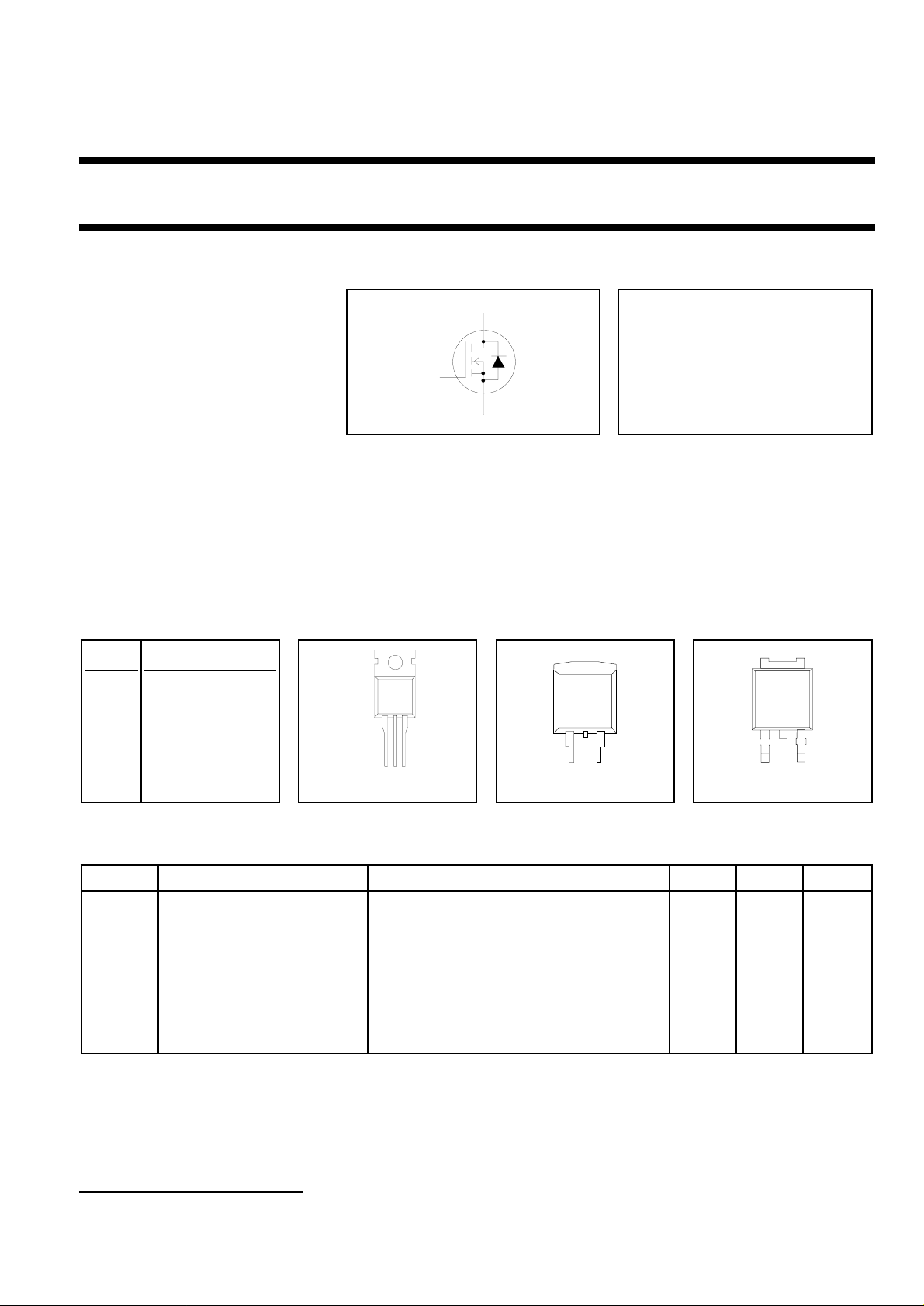
N-channel TrenchMOS transistor PHP9NQ20T, PHB9NQ20T
PHD9NQ20T
FEATURES SYMBOL QUICK REFERENCE DATA
• ’Trench’ technology
• Low on-state resistance V
d
= 200 V
DSS
• Fast switching
• Low thermal resistance I
g
s
R
DS(ON)
= 8.7 A
D
≤ 400 mΩ
GENERAL DESCRIPTION
N-channel, enhancement mode field-effect power transistor using Trench technology, intended for use in off-line
switchedmodepowersupplies, T.V. andcomputermonitorpowersupplies, d.c. tod.c.converters,motor control circuits
and general purpose switching applications.
The PHP9NQ20T is supplied in the SOT78 (TO220AB) conventional leaded package
The PHB9NQ20T is supplied in the SOT404 (D2PAK) surface mounting package
The PHD9NQ20T is supplied in the SOT428 (DPAK) surface mounting package
PINNING SOT78 (TO220AB) SOT404 (D2PAK) SOT428 (DPAK)
PIN DESCRIPTION
1 gate
2 drain
1
3 source
tab drain
tab
123
tab
2
13
tab
123
LIMITING VALUES
Limiting values in accordance with the Absolute Maximum System (IEC 134)
SYMBOL PARAMETER CONDITIONS MIN. MAX. UNIT
V
DSS
V
DGR
V
GS
I
D
I
DM
P
D
Tj, T
1 It is not possible to make connection to pin:2 of the SOT404 or SOT428 packages.
August 1999 1 Rev 1.100
Drain-source voltage Tj = 25 ˚C to 175˚C - 200 V
Drain-gate voltage Tj = 25 ˚C to 175˚C; RGS = 20 kΩ - 200 V
Gate-source voltage - ± 20 V
Continuous drain current Tmb = 25 ˚C; VGS = 10 V - 8.7 A
Tmb = 100 ˚C; VGS = 10 V - 6.2 A
Pulsed drain current Tmb = 25 ˚C - 35 A
Total power dissipation Tmb = 25 ˚C - 88 W
Operating junction and - 55 175 ˚C
stg
storage temperature

Philips Semiconductors Product specification
TrenchMOS transistor PHP9NQ20T, PHB9NQ20T
AVALANCHE ENERGY LIMITING VALUES
Limiting values in accordance with the Absolute Maximum System (IEC 134)
SYMBOL PARAMETER CONDITIONS MIN. MAX. UNIT
E
AS
I
AS
THERMAL RESISTANCES
SYMBOL PARAMETER CONDITIONS MIN. TYP. MAX. UNIT
R
th j-mb
R
th j-a
Non-repetitive avalanche Unclamped inductive load, IAS = 7.2A; - 93 mJ
energy tp = 100 µs; Tj prior to avalanche = 25˚C;
VDD ≤ 25 V; RGS = 50 Ω; VGS = 10 V; refer
to fig;15
Peak non-repetitive - 8.7 A
avalanche current
Thermal resistance junction - - 1.7 K/W
to mounting base
Thermal resistance junction SOT78 package, in free air - 60 - K/W
to ambient SOT404 & SOT428 packages, pcb - 50 - K/W
mounted, minimum footprint
ELECTRICAL CHARACTERISTICS
Tj= 25˚C unless otherwise specified
SYMBOL PARAMETER CONDITIONS MIN. TYP. MAX. UNIT
V
(BR)DSS
V
GS(TO)
R
DS(ON)
g
fs
I
GSS
I
DSS
Q
g(tot)
Q
gs
Q
gd
t
d on
t
r
t
d off
t
f
L
d
L
d
L
s
C
iss
C
oss
C
rss
Drain-source breakdown VGS = 0 V; ID = 0.25 mA; 200 - - V
voltage Tj = -55˚C 178 - - V
Gate threshold voltage VDS = VGS; ID = 1 mA 2 3 4 V
Tj = 175˚C 1 - - V
Tj = -55˚C - 6 V
Drain-source on-state VGS = 10 V; ID = 4.5 A - 300 400 mΩ
resistance Tj = 175˚C - - 1.16 Ω
Forward transconductance VDS = 25 V; ID = 4.5 A 3.8 6 - S
Gate source leakage current VGS = ± 10 V; VDS = 0 V - 10 100 nA
Zero gate voltage drain VDS = 200 V; VGS = 0 V - 0.05 10 µA
current Tj = 175˚C - - 500 µA
Total gate charge ID = 9 A; V
= 160 V; VGS = 10 V - 24 - nC
DD
Gate-source charge - 4 - nC
Gate-drain (Miller) charge - 12 - nC
Turn-on delay time VDD = 100 V; RD = 10 Ω;-8-ns
Turn-on rise time VGS = 10 V; RG = 5.6 Ω -19-ns
Turn-off delay time Resistive load - 25 - ns
Turn-off fall time - 15 - ns
Internal drain inductance Measured tab to centre of die - 3.5 - nH
Internal drain inductance Measured from drain lead to centre of die - 4.5 - nH
(SOT78 package only)
Internal source inductance Measured from source lead to source - 7.5 - nH
bond pad
Input capacitance VGS = 0 V; VDS = 25 V; f = 1 MHz - 959 - pF
Output capacitance - 93 - pF
Feedback capacitance - 54 - pF
August 1999 2 Rev 1.100

Philips Semiconductors Product specification
TrenchMOS transistor PHP9NQ20T, PHB9NQ20T
REVERSE DIODE LIMITING VALUES AND CHARACTERISTICS
Tj = 25˚C unless otherwise specified
SYMBOL PARAMETER CONDITIONS MIN. TYP. MAX. UNIT
I
S
I
SM
V
SD
t
rr
Q
rr
Continuous source current - - 9 A
(body diode)
Pulsed source current (body - - 36 A
diode)
Diode forward voltage IF = 9 A; VGS = 0 V - 0.85 1.2 V
Reverse recovery time IF = 9 A; -dIF/dt = 100 A/µs; - 92 - ns
Reverse recovery charge VGS = -10 V; VR = 25 V - 0.5 - µC
August 1999 3 Rev 1.100
Philips Semiconductors Product specification
TrenchMOS transistor PHP9NQ20T, PHB9NQ20T
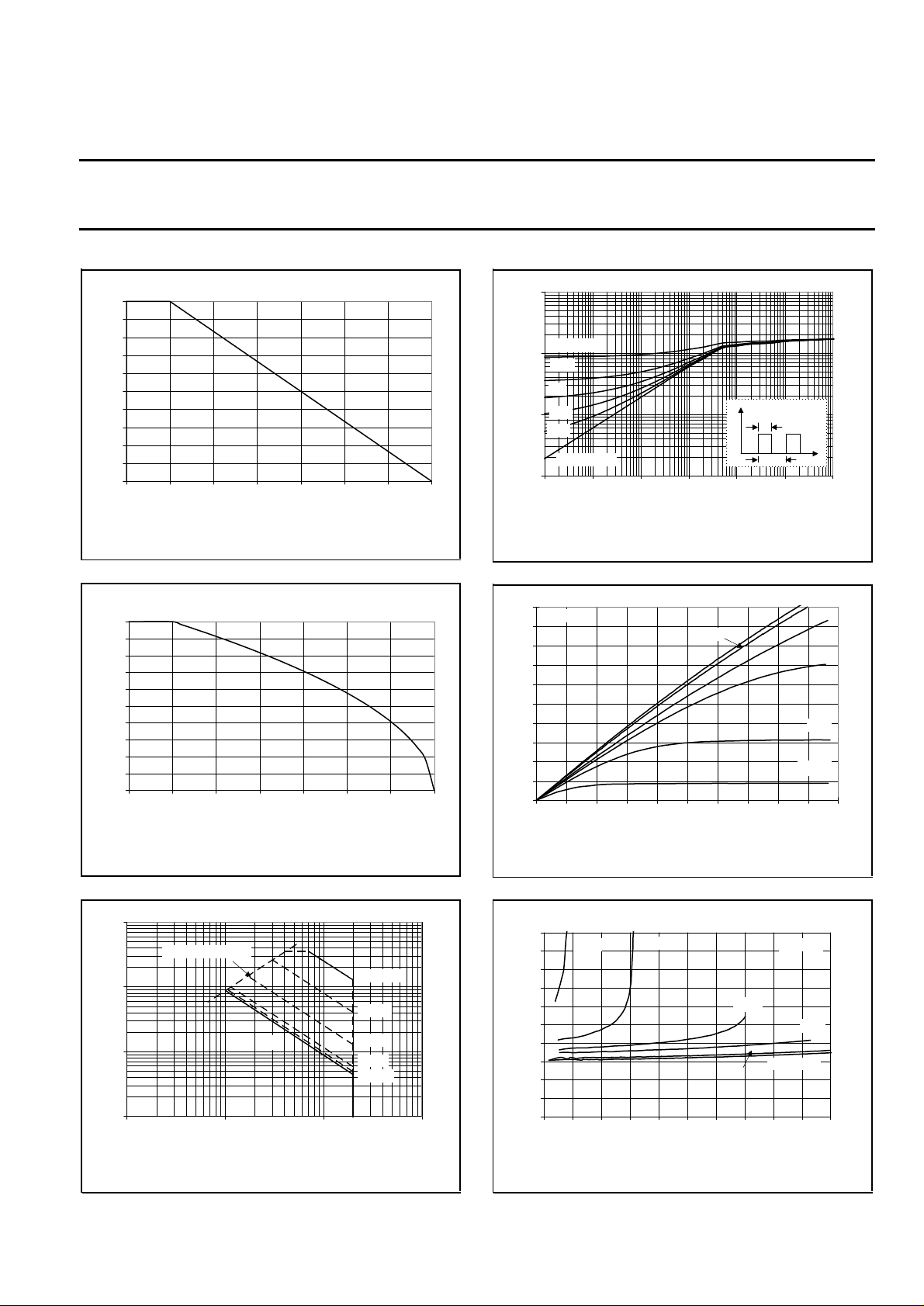
Normalised Power Derating, PD (%)
100
90
80
70
60
50
40
30
20
10
0
0 25 50 75 100 125 150 175
Mounting Base temperature, Tmb (C)
Fig.1. Normalised power dissipation.
PD% = 100⋅PD/P
Normalised Current Derating, ID (%)
100
90
80
70
60
50
40
30
20
10
0
0 25 50 75 100 125 150 175
Mounting Base temperature, Tmb (C)
D 25 ˚C
= f(Tmb)
Fig.2. Normalised continuous drain current.
ID% = 100⋅ID/I
= f(Tmb); VGS ≥ 10 V
D 25 ˚C
Transient thermal impedance, Zth j-mb (K/W)
10
D = 0.5
1
0.2
0.1
0.05
0.1
0.02
single pulse
0.01
1E-06 1E-05 1E-04 1E-03 1E-02 1E-01 1E+00
Pulse width, tp (s)
P
D
tp
D = tp/T
T
Fig.4. Transient thermal impedance.
Z
= f(t); parameter D = tp/T
th j-mb
Drain Current, ID (A)
10
Tj = 25 C VGS = 10V
9
8
7
6
5
4
3
2
1
0
0 0.2 0.4 0.6 0.8 1 1.2 1.4 1.6 1.8 2
Drain-Source Voltage, VDS (V)
8 V
6 V
5.5 V
5 V
4.5 V
Fig.5. Typical output characteristics, Tj = 25 ˚C
ID = f(VDS)
.
Peak Pulsed Drain Current, IDM (A)
100
RDS(on) = VDS/ ID
10
1
0.1
1 10 100 1000
Drain-Source Voltage, VDS (V)
D.C.
tp = 10 us
100 us
1 ms
10 ms
100 ms
Fig.3. Safe operating area
ID & IDM = f(VDS); IDM single pulse; parameter t
p
Drain-Source On Resistance, RDS(on) (Ohms)
0.5
0.45
0.4
0.35
0.3
0.25
0.2
0.15
0.1
0.05
4.5 V
0
012345678910
5 V
Drain Current, ID (A)
8 V
Tj = 25 C
5.5 V
6 V
VGS = 10V
Fig.6. Typical on-state resistance, Tj = 25 ˚C
R
= f(ID)
DS(ON)
.
August 1999 4 Rev 1.100
 Loading...