

Philips PHB8ND50E, PHW8ND50E, PHP8ND50E Datasheet
Philips Semiconductors Product specification
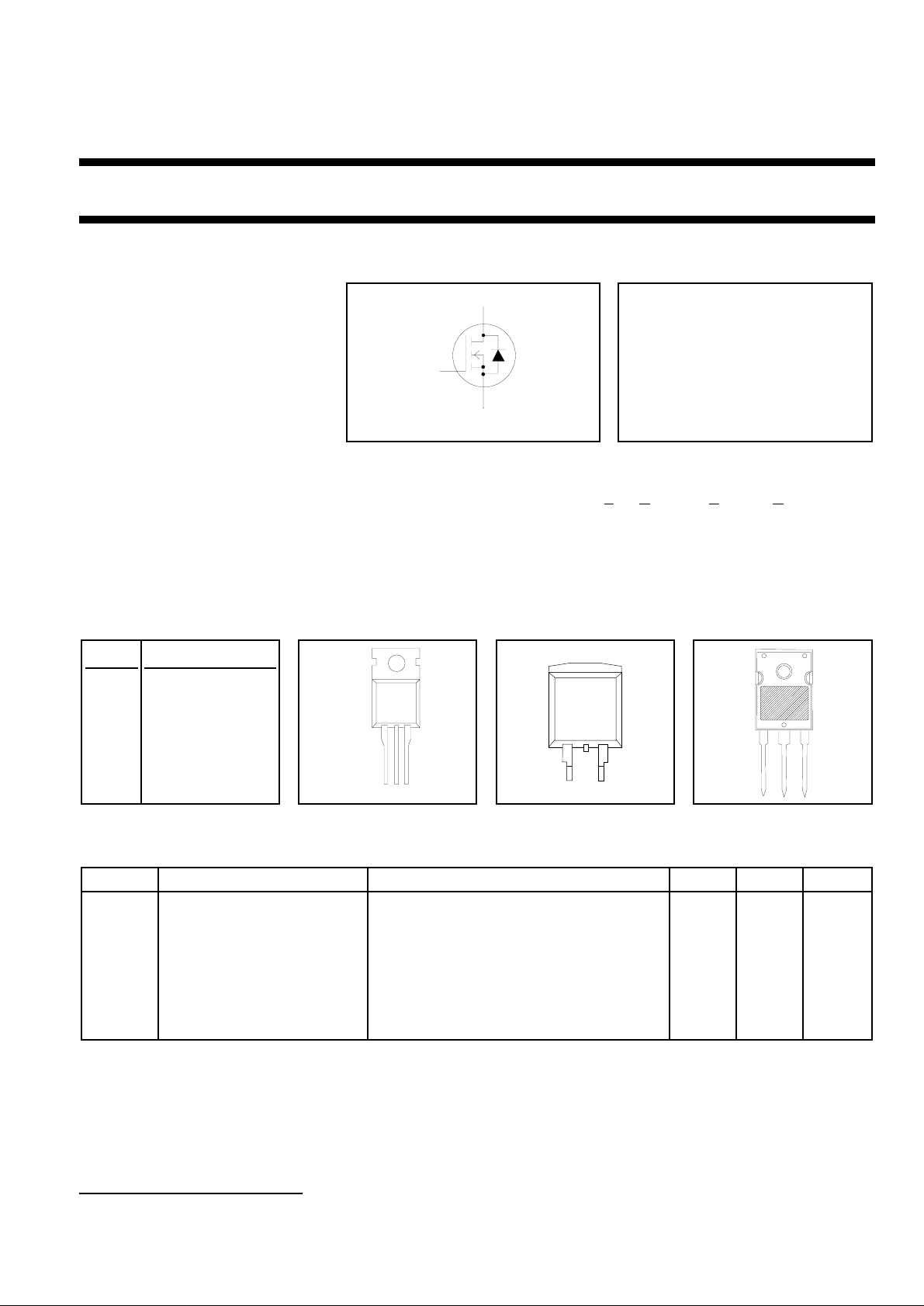
PowerMOS transistors PHP8ND50E, PHB8ND50E, PHW8ND50E
FREDFET, Avalanche energy rated
FEATURES SYMBOL QUICK REFERENCE DATA
• Repetitive Avalanche Rated V
d
= 500 V
DSS
• Fast switching
• Stable off-state characteristics I
• High thermal cycling performance
• Low thermal resistance R
g
= 8.5 A
D
DS(ON)
≤ 0.85 Ω
• Fast reverse recovery diode
s
trr = 180 ns
GENERAL DESCRIPTION
N-channel, enhancement mode field-effect power transistor, incorporating a Fast Recovery Epitaxial Diode (FRED).
This gives improved switching performance in half bridge and full bridge converters making this device particularly
suitable for inverters, lighting ballasts and motor control circuits.
The PHP8ND50E is supplied in the SOT78 (TO220AB) conventional leaded package.
The PHW8ND50E is supplied in the SOT429 (TO247) conventional leaded package.
The PHB8ND50E is supplied in the SOT404 surface mounting package.
PINNING SOT78 (TO220AB) SOT404 SOT429 (TO247)
PIN DESCRIPTION
1 gate
2 drain
1
tab
tab
3 source
2
tab drain
123
13
2
3
1
LIMITING VALUES
Limiting values in accordance with the Absolute Maximum System (IEC 134)
SYMBOL PARAMETER CONDITIONS MIN. MAX. UNIT
V
DSS
V
DGR
V
GS
I
D
I
DM
P
D
Tj, T
Drain-source voltage Tj = 25 ˚C to 150˚C - 500 V
Drain-gate voltage Tj = 25 ˚C to 150˚C; RGS = 20 kΩ - 500 V
Gate-source voltage - ± 30 V
Continuous drain current Tmb = 25 ˚C; VGS = 10 V - 8.5 A
Tmb = 100 ˚C; VGS = 10 V - 5.4 A
Pulsed drain current Tmb = 25 ˚C - 34 A
Total dissipation Tmb = 25 ˚C - 147 W
Operating junction and - 55 150 ˚C
stg
storage temperature range
1 It is not possible to make connection to pin 2 of the SOT404 package.
August 1998 1 Rev 1.100

Philips Semiconductors Product specification
PowerMOS transistors PHP8ND50E, PHB8ND50E, PHW8ND50E
FREDFET, Avalanche energy rated
AVALANCHE ENERGY LIMITING VALUES
Limiting values in accordance with the Absolute Maximum System (IEC 134)
SYMBOL PARAMETER CONDITIONS MIN. MAX. UNIT
E
AS
E
AR
IAS, I
THERMAL RESISTANCES
SYMBOL PARAMETER CONDITIONS MIN. TYP. MAX. UNIT
R
th j-mb
R
th j-a
Non-repetitive avalanche Unclamped inductive load, IAS = 6.2 A; - 510 mJ
energy tp = 0.18 ms; Tj prior to avalanche = 25˚C;
VDD ≤ 50 V; RGS = 50 Ω; VGS = 10 V; refer
to fig:17
Repetitive avalanche energy2IAR = 8.5 A; tp = 1 µs; Tj prior to - 19 mJ
avalanche = 25˚C; RGS = 50 Ω; VGS = 10 V;
refer to fig:18
Repetitive and non-repetitive - 8.5 A
AR
avalanche current
Thermal resistance junction - - 0.85 K/W
to mounting base
Thermal resistance junction SOT78 package, in free air - 60 - K/W
to ambient SOT429 package, in free air - 45 - K/W
SOT404 package, pcb mounted, minimum - 50 - K/W
footprint
2 pulse width and repetition rate limited by Tj max.
August 1998 2 Rev 1.100

Philips Semiconductors Product specification
PowerMOS transistors PHP8ND50E, PHB8ND50E, PHW8ND50E
FREDFET, Avalanche energy rated
ELECTRICAL CHARACTERISTICS
Tj = 25 ˚C unless otherwise specified
SYMBOL PARAMETER CONDITIONS MIN. TYP. MAX. UNIT
V
(BR)DSS
∆V
∆T
R
DS(ON)
V
GS(TO)
g
fs
I
DSS
I
GSS
Q
g(tot)
Q
gs
Q
gd
t
d(on)
t
r
t
d(off)
t
f
L
d
L
d
L
s
C
iss
C
oss
C
rss
(BR)DSS
j
Drain-source breakdown VGS = 0 V; ID = 0.25 mA 500 - - V
voltage
/ Drain-source breakdown VDS = VGS; ID = 0.25 mA - 0.1 - %/K
voltage temperature
coefficient
Drain-source on resistance VGS = 10 V; ID = 4.8 A - 0.7 0.85 Ω
Gate threshold voltage VDS = VGS; ID = 0.25 mA 2.0 3.0 4.0 V
Forward transconductance VDS = 30 V; ID = 4.8 A 3.5 6 - S
Drain-source leakage current VDS = 500 V; VGS = 0 V - 1 25 µA
VDS = 400 V; VGS = 0 V; Tj = 125 ˚C - 40 250 µA
Gate-source leakage current VGS = ±30 V; VDS = 0 V - 10 200 nA
Total gate charge ID = 8.5 A; V
= 400 V; VGS = 10 V - 88 110 nC
DD
Gate-source charge - 6 7 nC
Gate-drain (Miller) charge - 47 60 nC
Turn-on delay time VDD = 250 V; RD = 30 Ω; - 18 - ns
Turn-on rise time RG = 9.1 Ω -50-ns
Turn-off delay time - 104 - ns
Turn-off fall time - 60 - ns
Internal drain inductance Measured from tab to centre of die - 3.5 - nH
Internal drain inductance Measured from drain lead to centre of die - 4.5 - nH
(SOT78 and SOT429 packages only)
Internal source inductance Measured from source lead to source - 7.5 - nH
bond pad
Input capacitance VGS = 0 V; VDS = 25 V; f = 1 MHz - 1060 - pF
Output capacitance - 160 - pF
Feedback capacitance - 90 - pF
SOURCE-DRAIN DIODE RATINGS AND CHARACTERISTICS
Tj = 25 ˚C unless otherwise specified
SYMBOL PARAMETER CONDITIONS MIN. TYP. MAX. UNIT
I
S
I
SM
V
SD
t
rr
Q
rr
I
rrm
Continuous source current Tmb = 25˚C - - 8.5 A
(body diode)
Pulsed source current (body Tmb = 25˚C - - 34 A
diode)
Diode forward voltage IS = 8.5 A; VGS = 0 V - - 1.5 V
Reverse recovery time IS = 8.5 A; VGS = 0 V; dI/dt = 100 A/µs - 180 - ns
IS = 8.5 A; VGS = 0 V; dI/dt = 100 A/µs; - 220 - ns
125˚C
Reverse recovery charge IS = 8.5 A; VGS = 0 V; dI/dt = 100 A/µs - 0.65 - µC
IS = 8.5 A; VGS = 0 V; dI/dt = 100 A/µs; - 2.6 - µC
125˚C
Peak reverse recovery IS = 8.5 A; VGS = 0 V; dI/dt = 100 A/µs; - 15 - A
current 125˚C
August 1998 3 Rev 1.100
 Loading...