

Philips PHB7N60E, PHP7N60E, PHW7N60E Datasheet
Philips Semiconductors Product specification
PowerMOS transistors PHP7N60E, PHB7N60E, PHW7N60E
Avalanche energy rated
FEATURES SYMBOL QUICK REFERENCE DATA
• Repetitive Avalanche Rated
• Fast switching V
d
= 600 V
DSS
• Stable off-state characteristics
• High thermal cycling performance I
• Low thermal resistance
g
s
R
DS(ON)
= 7 A
D
≤ 1.2 Ω
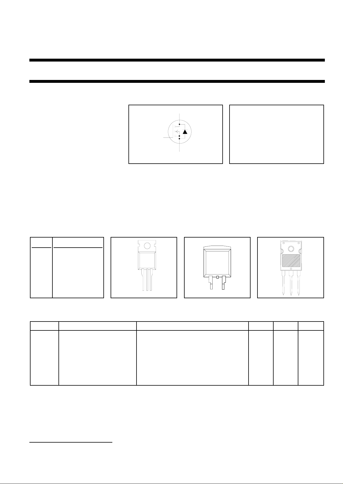
GENERAL DESCRIPTION
N-channel,enhancementmodefield-effect power transistor, intendedforusein off-line switched mode powersupplies,
T.V.andcomputer monitor powersupplies, d.c. to d.c.converters, motor controlcircuitsand general purpose switching
applications.
The PHP7N60E is supplied in the SOT78 (TO220AB) conventional leaded package.
The PHW7N60E is supplied in the SOT429 (TO247) conventional leaded package.
The PHB7N60E is supplied in the SOT404 surface mounting package.
PINNING SOT78 (TO220AB) SOT404 SOT429 (TO247)
PIN DESCRIPTION
1 gate
2 drain
1
tab
tab
3 source
2
tab drain
123
13
2
3
1
LIMITING VALUES
Limiting values in accordance with the Absolute Maximum System (IEC 134)
SYMBOL PARAMETER CONDITIONS MIN. MAX. UNIT
V
DSS
V
DGR
V
GS
I
D
I
DM
P
D
Tj, T
Drain-source voltage Tj = 25 ˚C to 150˚C - 600 V
Drain-gate voltage Tj = 25 ˚C to 150˚C; RGS = 20 kΩ - 600 V
Gate-source voltage - ± 30 V
Continuous drain current Tmb = 25 ˚C; VGS = 10 V - 7 A
Tmb = 100 ˚C; VGS = 10 V - 4.5 A
Pulsed drain current Tmb = 25 ˚C - 28 A
Total dissipation Tmb = 25 ˚C - 147 W
Operating junction and - 55 150 ˚C
stg
storage temperature range
1 It is not possible to make connection to pin 2 of the SOT404 package.
December 1998 1 Rev 1.400
Philips Semiconductors Product specification
PowerMOS transistors PHP7N60E, PHB7N60E, PHW7N60E
Avalanche energy rated
AVALANCHE ENERGY LIMITING VALUES
Limiting values in accordance with the Absolute Maximum System (IEC 134)
SYMBOL PARAMETER CONDITIONS MIN. MAX. UNIT
E
AS
E
AR
IAS, I
THERMAL RESISTANCES
SYMBOL PARAMETER CONDITIONS MIN. TYP. MAX. UNIT
R
th j-mb
R
th j-a
Non-repetitive avalanche Unclamped inductive load, IAS = 6.5 A; - 583 mJ
energy tp = 0.23 ms; Tj prior to avalanche = 25˚C;
VDD ≤ 50 V; RGS = 50 Ω; VGS = 10 V; refer
to fig:17
Repetitive avalanche energy2IAR = 7 A; tp = 2.5 µs; Tj prior to - 13 mJ
avalanche = 25˚C; RGS = 50 Ω; VGS = 10 V;
refer to fig:18
Repetitive and non-repetitive - 7 A
AR
avalanche current
Thermal resistance junction - - 0.85 K/W
to mounting base
Thermal resistance junction SOT78 package, in free air - 60 - K/W
to ambient SOT429 package, in free air - 45 - K/W
SOT404 package, pcb mounted, minimum - 50 - K/W
footprint
2 pulse width and repetition rate limited by Tj max.
December 1998 2 Rev 1.400
Philips Semiconductors Product specification
PowerMOS transistors PHP7N60E, PHB7N60E, PHW7N60E
Avalanche energy rated
ELECTRICAL CHARACTERISTICS
Tj = 25 ˚C unless otherwise specified
SYMBOL PARAMETER CONDITIONS MIN. TYP. MAX. UNIT
V
(BR)DSS
∆V
∆T
R
DS(ON)
V
GS(TO)
g
fs
I
DSS
I
GSS
Q
g(tot)
Q
gs
Q
gd
t
d(on)
t
r
t
d(off)
t
f
L
d
L
d
L
s
C
iss
C
oss
C
rss
(BR)DSS
j
Drain-source breakdown VGS = 0 V; ID = 0.25 mA 600 - - V
voltage
/ Drain-source breakdown VDS = VGS; ID = 0.25 mA - 0.1 - %/K
voltage temperature
coefficient
Drain-source on resistance VGS = 10 V; ID = 3.5 A - 0.9 1.2 Ω
Gate threshold voltage VDS = VGS; ID = 0.25 mA 2.0 3.0 4.0 V
Forward transconductance VDS = 30 V; ID = 3.5 A 3 4.5 - S
Drain-source leakage current VDS = 600 V; VGS = 0 V - 2 100 µA
VDS = 480 V; VGS = 0 V; Tj = 125 ˚C - 50 500 µA
Gate-source leakage current VGS = ±30 V; VDS = 0 V - 10 200 nA
Total gate charge ID = 7 A; V
= 480 V; VGS = 10 V - 54 80 nC
DD
Gate-source charge - 5.5 7 nC
Gate-drain (Miller) charge - 30 45 nC
Turn-on delay time VDD = 300 V; RD = 39 Ω; - 17 - ns
Turn-on rise time RG = 9.1 Ω -31-ns
Turn-off delay time - 88 - ns
Turn-off fall time - 34 - ns
Internal drain inductance Measured from tab to centre of die - 3.5 - nH
Internal drain inductance Measured from drain lead to centre of die - 4.5 - nH
(SOT78 and SOT429 packages only)
Internal source inductance Measured from source lead to source - 7.5 - nH
bond pad
Input capacitance VGS = 0 V; VDS = 25 V; f = 1 MHz - 930 - pF
Output capacitance - 120 - pF
Feedback capacitance - 70 - pF
SOURCE-DRAIN DIODE RATINGS AND CHARACTERISTICS
Tj = 25 ˚C unless otherwise specified
SYMBOL PARAMETER CONDITIONS MIN. TYP. MAX. UNIT
I
S
I
SM
V
SD
t
rr
Q
rr
Continuous source current Tmb = 25˚C - - 7 A
(body diode)
Pulsed source current (body Tmb = 25˚C - - 28 A
diode)
Diode forward voltage IS = 7 A; VGS = 0 V - - 1.2 V
Reverse recovery time IS = 7 A; VGS = 0 V; dI/dt = 100 A/µs - 530 - ns
Reverse recovery charge - 6.7 - µC
December 1998 3 Rev 1.400
 Loading...