

Philips PHP71NQ03LT, PHB71NQ03LT, PHD71NQ03LT User Guide
1. Product profile
1.1 Description
1.2 Features
PHP/PHB/PHD71NQ03LT
TrenchMOS™ logic level FET
Rev. 01 — 25 June 2002 Product data
N-channel enhancement mode field-effect transistor in a plastic package using
TrenchMOS™ technology.
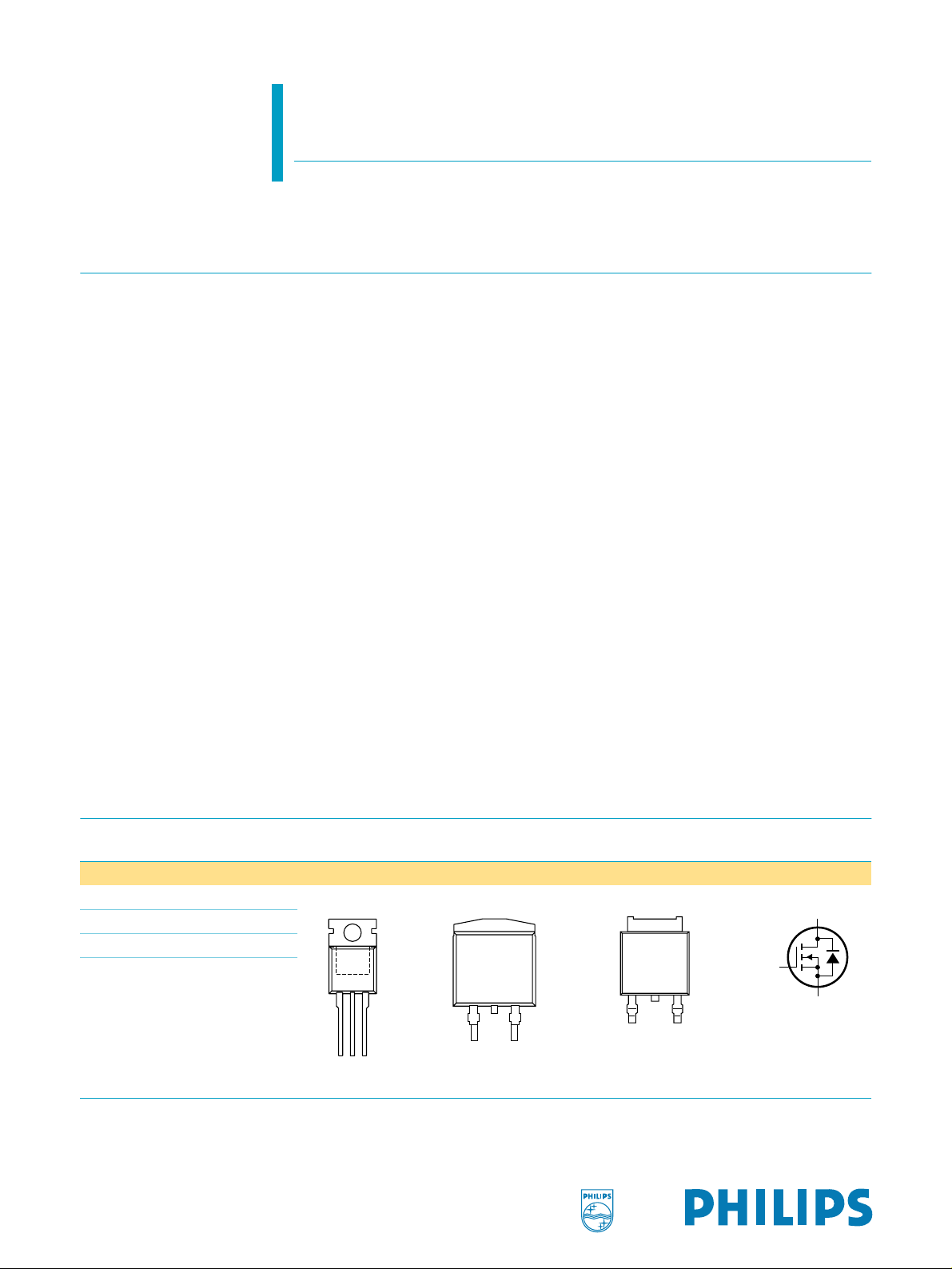
Product availability:
PHP71NQ03LT in SOT78 (TO-220AB)
PHB71NQ03LT in SOT404 (D2-PAK)
PHD71NQ03LT in SOT428 (D-PAK).
■ Logic level compatible ■ Low gate charge
1.3 Applications
■ DC to DC converters ■ Switched mode power supplies
1.4 Quick reference data
■ VDS=30V ■ ID=75A
■ P
= 120 W ■ R
tot
DSon
≤ 10 mΩ
2. Pinning information
Table 1: Pinning - SOT78, SOT404, SOT428 simplified outline and symbol
Pin Description Simplified outline Symbol
1 gate (g)
2 drain (d)
3 source (s)
mb mounting base,
connected to drain (d)
[1]
MBK106
12mb3
SOT78 (TO-220) SOT404 (D
mb
2
13
MBK116
2
-PAK) SOT428 (D-PAK)
mb
2
13
Top view
MBK091
MBB076
d
g
s
[1] It is not possible to make connection to pin 2 of the SOT404 or SOT428 packages.

Philips Semiconductors
PHP/PHB/PHD71NQ03LT
TrenchMOS™ logic level FET
3. Limiting values
Table 2: Limiting values
In accordance with the Absolute Maximum Rating System (IEC 60134).
Symbol Parameter Conditions Min Max Unit
V
DS
V
DGR
V
GS
V
GSM
I
D
I
DM
P
tot
T
stg
T
j
Source-drain diode
I
S
I
SM
drain-source voltage (DC) 25 °C ≤ Tj≤ 175 °C - 30 V
drain-gate voltage (DC) 25 °C ≤ Tj≤ 175 °C; RGS=20kΩ -30V
gate-source voltage (DC) - ±20 V
peak gate-source voltage tp≤ 50 µs; pulsed; duty cycle = 25 % - ±25 V
drain current (DC) Tmb=25°C; VGS=10V;Figure 2 and 3 -75A
= 100 °C; VGS=10V;Figure 2 - 57.7 A
T
mb
peak drain current Tmb=25°C; pulsed; tp≤ 10 µs; Figure 3 - 240 A
total power dissipation Tmb=25°C; Figure 1 - 120 W
storage temperature −55 +175 °C
junction temperature −55 +175 °C
source (diode forward) current (DC) Tmb=25°C - 75 A
peak source (diode forward) current Tmb=25°C; pulsed; tp≤ 10 µs - 57.7 A
9397 750 09821
Product data Rev. 01 — 25 June 2002 2 of 14
© Koninklijke Philips Electronics N.V. 2002. All rights reserved.
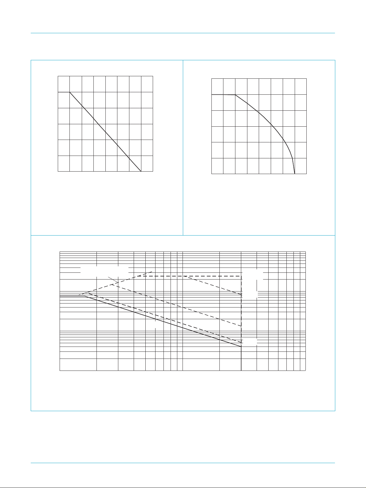
Philips Semiconductors
03aa16
0
40
80
120
0 50 100 150 200
Tmb (°C)
P
der
(%)
PHP/PHB/PHD71NQ03LT
TrenchMOS™ logic level FET
P
tot
P
der
-----------------------
P
tot 25 C°()
100%×= I
Fig 1. Normalized total power dissipation as a
function of mounting base temperature.
3
10
120
I
der
(%)
80
40
0
0 50 100 150 200
I
D
der
-------------------
I
D25C
()
100%×=
°
03ai74
Tmb (°C)
Fig 2. Normalized continuous drain current as a
function of mounting base temperature.
03ai76
I
D
(A)
2
10
10
1
1 10 10
Limit R
DSon
= V
DS
/ I
D
DC
tp = 10 µs
100 µs
1 ms
10 ms
2
VDS (V)
Tmb=25°C; IDM is single pulse; VGS = 10V.
Fig 3. Safe operating area; continuous and peak drain currents as a function of drain-source voltage.
9397 750 09821
Product data Rev. 01 — 25 June 2002 3 of 14
© Koninklijke Philips Electronics N.V. 2002. All rights reserved.
Philips Semiconductors
PHP/PHB/PHD71NQ03LT
TrenchMOS™ logic level FET
4. Thermal characteristics
Table 3: Thermal characteristics
Symbol Parameter Conditions Min Typ Max Unit
R
th(j-mb)
R
th(j-a)
thermal resistance from junction to mounting base Figure 4 - - 1.25 K/W
thermal resistance from junction to ambient
SOT78 vertical in still air - 60 - K/W
SOT428 SOT428 minimum footprint;
- 75 - K/W
mounted on a PCB
SOT404 and SOT428 SOT404 minimum footprint;
- 50 - K/W
mounted on a PCB
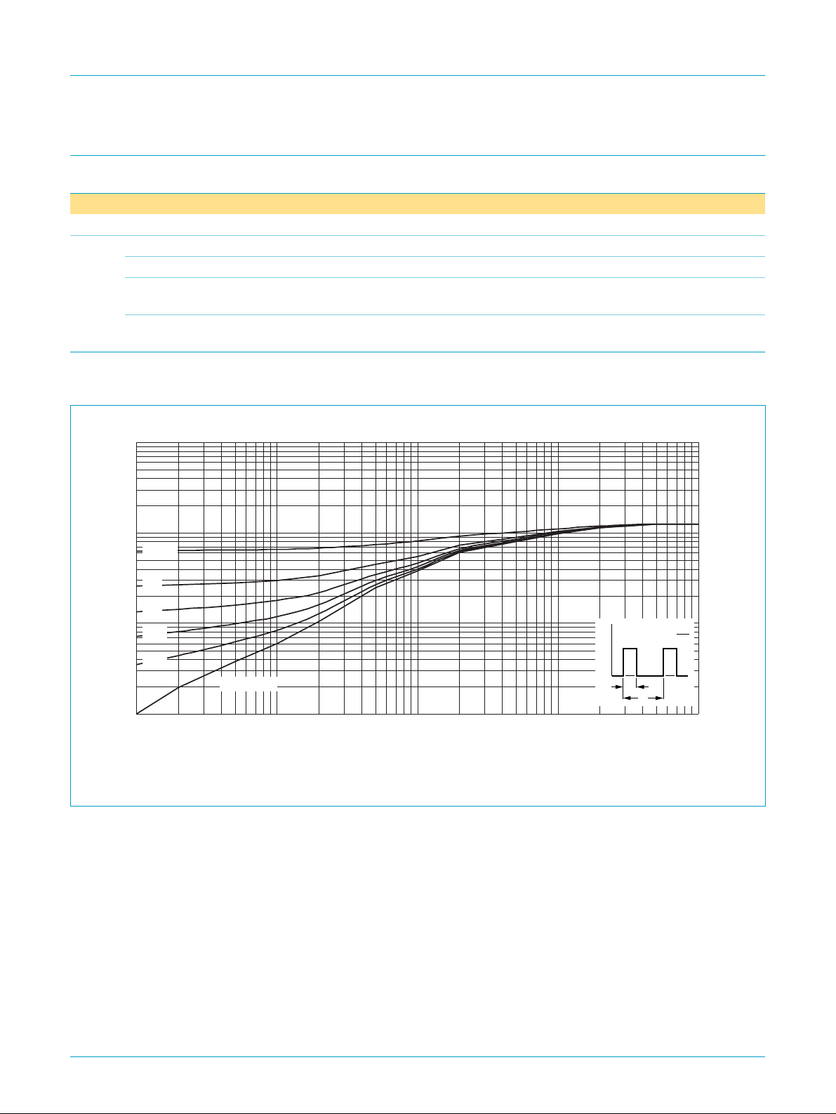
4.1 Transient thermal impedance
03ai75
δ =
t
p
T
tp (s)
Z
th(j-mb)
(K/W)
10
1
10
10
δ = 0.5
0.2
0.1
-1
0.05
0.02
single pulse
-2
10
-5
10
-4
10
-3
10
P
-2
Fig 4. Transient thermal impedance from junction to mounting base as a function of pulse duration.
t
p
T
t
-1
10
9397 750 09821
© Koninklijke Philips Electronics N.V. 2002. All rights reserved.
Product data Rev. 01 — 25 June 2002 4 of 14

Philips Semiconductors
PHP/PHB/PHD71NQ03LT
TrenchMOS™ logic level FET
5. Characteristics
Table 4: Characteristics
Tj=25°C unless otherwise specified
Symbol Parameter Conditions Min Typ Max Unit
Static characteristics
V
(BR)DSS
V
GS(th)
I
DSS
I
GSS
R
DSon
Dynamic characteristics
Q
g(tot)
Q
gs
Q
gd
C
iss
C
oss
C
rss
t
d(on)
t
r
t
d(off)
t
f
Source-drain diode
V
SD
t
rr
Q
r
drain-source breakdown voltage ID= 250 µA; VGS=0V
T
=25°C 30--V
j
= −55 °C 27--V
T
j
gate-source threshold voltage ID= 1 mA; VDS=VGS; Figure 9
T
=25°C 1 1.9 2.5 V
j
= 175 °C 0.6 - - V
T
j
= −55 °C - - 2.9 V
T
j
drain-source leakage current VDS=30V; VGS=0V
T
=25°C - 0.05 1 µA
j
= 175 °C - - 500 µA
T
j
gate-source leakage current VGS= ±20 V; VDS= 0 V - 10 100 nA
drain-source on-state resistance VGS=5V; ID=25A;Figure 7 and 8
T
=25°C - 12 15.2 mΩ
j
= 175 °C - 21.6 27.4 mΩ
T
j
= 10 V; ID=25A;Figure 7 - 8 10 mΩ
V
GS
total gate charge ID= 50 A; VDD=15V; VGS=5V;Figure 13 - 13.2 - nC
gate-source charge - 5.3 - nC
gate-drain (Miller) charge - 4.6 - nC
input capacitance VGS=0V; VDS= 25 V; f = 1 MHz; Figure 11 - 1220 - pF
output capacitance - 330 - pF
reverse transfer capacitance - 140 - pF
turn-on delay time VDD=15V; ID= 25 A; VGS= 4.5 V; RG= 5.6 Ω -15-ns
rise time - 150 - ns
turn-off delay time - 13.5 - ns
fall time -18-ns
source-drain (diode forward) voltage IS= 25 A; VGS=0V;Figure 12 - 0.9 1.2 V
reverse recovery time IS= 10 A; dIS/dt = −100 A/µs; VGS=0V - 29 - ns
recovered charge - 20 - nC
9397 750 09821
Product data Rev. 01 — 25 June 2002 5 of 14
© Koninklijke Philips Electronics N.V. 2002. All rights reserved.
 Loading...