

Philips PHB47NQ10T, PHP47NQ10T Datasheet

1. Description
2. Features
PHP47NQ10T; PHB47NQ10T
N-channel enhancement mode field-effect transistor
Rev. 01 — 16 May 2001 Product data
N-channel enhancement mode field-effect powertransistorina plastic package using
TrenchMOS™1 technology.
Product availability:
PHP47NQ10T in SOT78 (TO-220AB)
PHB47NQ10T in SOT404 (D2-PAK).
■ Fast switching
■ Very low on-state resistance.
3. Applications
■ DC to DC converters
■ Switched mode power supplies.
c
4. Pinning information
Table 1: Pinning - SOT78 and SOT404, simplified outline and symbol
Pin Description Simplified outline Symbol
1 gate (g)
2 drain (d)
3 source (s)
mb mounting base;
[1] It is not possible to make connection to pin 2 of the SOT404 package.
c
connected to
drain (d)
[1]
12mb3
SOT78 (TO-220AB)
MBK106
mb
2
13
SOT404 (D
MBK116
2
-PAK)
g
MBB076
d
s
1. TrenchMOS is a trademark of Royal Philips Electronics.

Philips Semiconductors
PHP47NQ10T; PHB47NQ10T
N-channel enhancement mode field-effect transistor
5. Quick reference data
Table 2: Quick reference data
Symbol Parameter Conditions Typ Max Unit
V
I
P
T
R
DS
D
tot
j
DSon
drain-source voltage (DC) Tj=25to175°C − 100 V
drain current (DC) Tmb=25°C; VGS=10V − 47 A
total power dissipation Tmb=25°C − 166 W
junction temperature − 175 °C
drain-source on-state resistance Tj=25°C; VGS=10V; ID= 25 A 20 28 mΩ
6. Limiting values
Table 3: Limiting values
In accordance with the Absolute Maximum Rating System (IEC 60134).
Symbol Parameter Conditions Min Max Unit
V
DS
V
DGR
V
GS
I
D
I
DM
P
tot
T
stg
T
j
Source-drain diode
I
S
I
SM
Avalanche ruggedness
E
AS
drain-source voltage (DC) Tj=25to175°C − 100 V
drain-gate voltage (DC) Tj=25to175°C; RGS=20kΩ−100 V
gate-source voltage (DC) −±20 V
drain current (DC) Tmb=25°C; VGS=10V
− 47 A
Figure 2 and 3
T
= 100 °C; VGS=10V
mb
− 33 A
Figure 2
peak drain current Tmb=25°C; pulsed; tp≤ 10 µs;
− 187 A
Figure 3
total power dissipation Tmb=25°C; Figure 1 − 166 W
storage temperature −55 175 °C
operating junction temperature −55 175 °C
source (diode forward) current
Tmb=25°C − 47 A
(DC)
peak source (diode forward)
Tmb=25°C; pulsed; tp≤ 10 µs − 187 A
current
non-repetitive avalanche energy unclamped inductive load;
= 30 A; tp= 0.1 ms; VDD≤ 25 V;
I
AS
=50Ω; VGS= 5 V; starting
R
GS
=25°C; Figure 4
T
j
− 45 mJ
9397 750 08243
Product data Rev. 01 — 16 May 2001 2 of 14
© Philips Electronics N.V. 2001. All rights reserved.
Philips Semiconductors
PHP47NQ10T; PHB47NQ10T
N-channel enhancement mode field-effect transistor
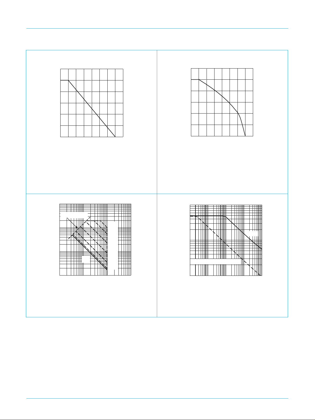
120
P
der
(%)
100
80
60
40
20
0
0 50 100 150 200
P
P
der
tot
----------------------
P
tot 25 C°()
100%×=
03aa16
T
(oC)
mb
Fig 1. Normalized total power dissipation as a
function of mounting base temperature.
tp =
1 µs
10 µs
100 µs
1 ms
10 ms
100ms
003aaa097
VDS (V)
10
3
10
I
D
R
= VDS / I
DSon
(A)
2
10
10
1
110102
D
D.C.
120
I
der
(%)
100
80
60
40
20
0
0 50 100 150 200
03aa24
T
(oC)
mb
VGS≥ 10 V
I
I
der
D
------------------ -
I
D25C°()
100%×=
Fig 2. Normalized continuous drain current as a
function of mounting base temperature.
1
003aaa098
25 oC
tp (ms)
10
2
10
I
AS
(A)
10
Tj prior to avalanche = 150 oC
3
1
-3
10
-2
10
-1
10
Tmb=25°C; IDM is single pulse. Unclamped inductive load; VDD≤ 25 V; RGS=50Ω;
VGS= 5 V; starting Tj=25°C and 150 °C.
Fig 3. Safe operating area; continuous and peak drain
currents as a function of drain-source voltage.
9397 750 08243
Fig 4. Non-repetitive avalanche ruggedness current
as a function of pulse duration.
© Philips Electronics N.V. 2001. All rights reserved.
Product data Rev. 01 — 16 May 2001 3 of 14
Philips Semiconductors
PHP47NQ10T; PHB47NQ10T
N-channel enhancement mode field-effect transistor
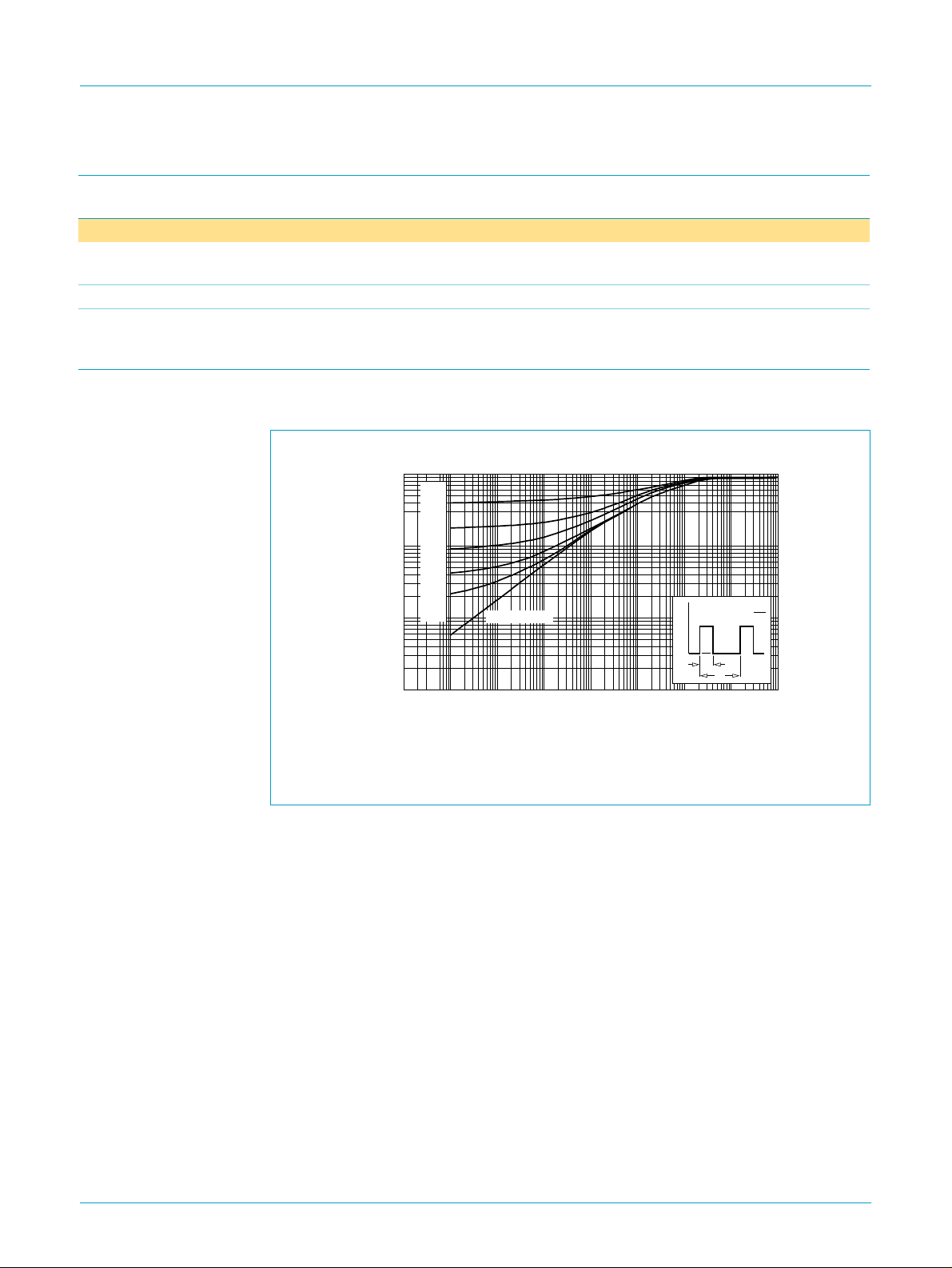
7. Thermal characteristics
Table 4: Thermal characteristics
Symbol Parameter Conditions Value Unit
R
th(j-mb)
R
th(j-a)
R
th(j-a)
thermal resistance from junction to mounting
base
thermal resistance from junction to ambient SOT78 package; vertical in still air. 60 K/W
thermal resistance from junction to ambient SOT404 package; mounted on
7.1 Transient thermal impedance
Figure 5 0.9 K/W
50 K/W
printed circuit board; minimum
footprint.
003aaa099
t
p
δ =
T
t
p
t
T
101
tp (s)
Z
th (j-mb)
(K/W)
10
1
δ =
0.5
0.2
-1
10
10
0.1
0.05
0.02
-2
-3
-7
10
Single pulse
-6
10
10
10
-4
-5
-3
10
P
-1
-2
10
10
Fig 5. Transient thermal impedance from junction to mounting base as a function of
pulse duration.
9397 750 08243
© Philips Electronics N.V. 2001. All rights reserved.
Product data Rev. 01 — 16 May 2001 4 of 14

Philips Semiconductors
PHP47NQ10T; PHB47NQ10T
N-channel enhancement mode field-effect transistor
8. Characteristics
Table 5: Characteristics
Tj=25°C unless otherwise specified
Symbol Parameter Conditions Min Typ Max Unit
Static characteristics
V
(BR)DSS
drain-source breakdown
voltage
V
I
DSS
I
GSS
R
GS(th)
DSon
gate-source threshold voltage ID= 1 mA; VDS=VGS;
drain-source leakage current VGS=0V; VDS= 100 V
gate-source leakage current VDS=0V; VGS= ±20 V − 2 100 nA
drain-source on-state
resistance
Dynamic characteristics
Q
Q
Q
C
C
C
t
d(on)
t
r
t
d(off)
t
f
g(tot)
gs
gd
iss
oss
rss
total gate charge ID= 40 A; VDD=80V;
gate-source charge − 12 − nC
gate-drain (Miller) charge − 21 − nC
input capacitance VGS=0V; VDS=25V;
output capacitance − 315 378 pF
reverse transfer capacitance − 187 256 pF
turn-on delay time VDD= 30 V; RD= 1.2 Ω;
rise time − 70 105 ns
turn-off delay time − 83 116 ns
fall time − 45 63 ns
Source-drain diode
V
SD
source-drain (diode forward)
voltage
t
rr
Q
r
reverse recovery time IS=47A;
recovered charge − 0.24 −µC
ID= 250 µA; VGS=0V 100 −−V
Figure 10
=25°C234V
T
j
= 175 °C1−−V
T
j
=25°C − 0.05 10 µA
T
j
= 175 °C −−500 µA
T
j
VGS=10V; ID=25A;
Figure 8 and 9
=25oC − 20 28 mΩ
T
j
= 175 °C −−76 mΩ
T
j
− 66 − nC
=10V;Figure 15
V
GS
− 2320 3100 pF
f = 1 MHz; Figure 13
− 15 23 ns
=10V; RG=10Ω
V
GS
IS= 25 A; VGS=0V;
− 0.85 1.2 V
Figure 14
− 66 − ns
/dt = −100 A/µs;
dI
S
= -10 V; VR=30V
V
GS
9397 750 08243
Product data Rev. 01 — 16 May 2001 5 of 14
© Philips Electronics N.V. 2001. All rights reserved.
 Loading...