

Philips phb125n06l DATASHEETS
Philips Semiconductors Product specification
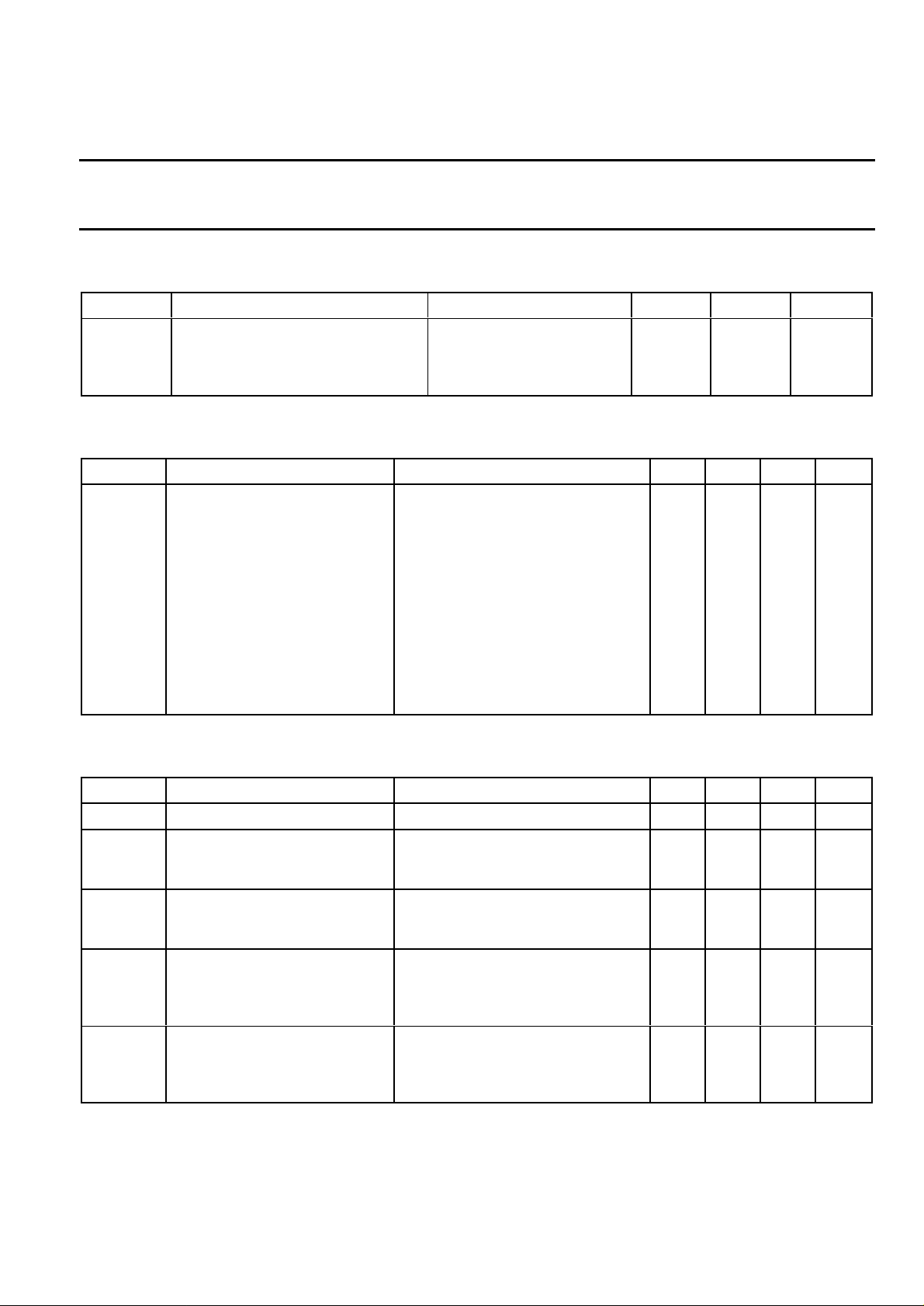
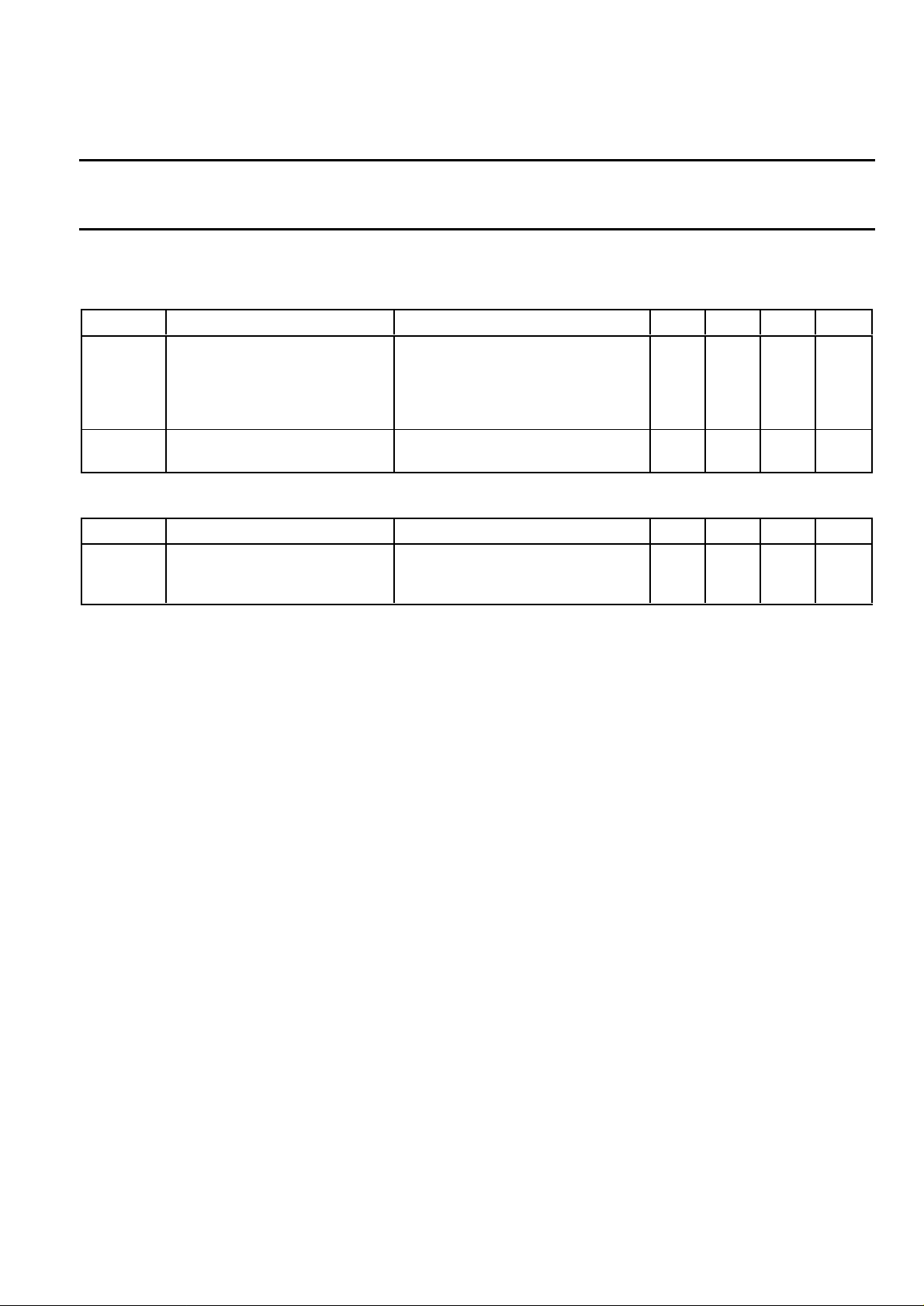
TrenchMOS transistor PHB125N06LT
Logic level FET
GENERAL DESCRIPTION QUICK REFERENCE DATA
N-channel enhancement mode logic SYMBOL PARAMETER MAX. UNIT
level field-effectpowertransistorina
plastic envelope suitable for surface V
mounting Using ’trench’ technology I
thedevice features very low on-state P
resistance and has integral zener T
diodes giving ESD protection up to R
DS
D
tot
j
DS(ON)
2kV. It is intended for use in DC-DC resistance VGS = 5 V
converters and general purpose
switching applications.
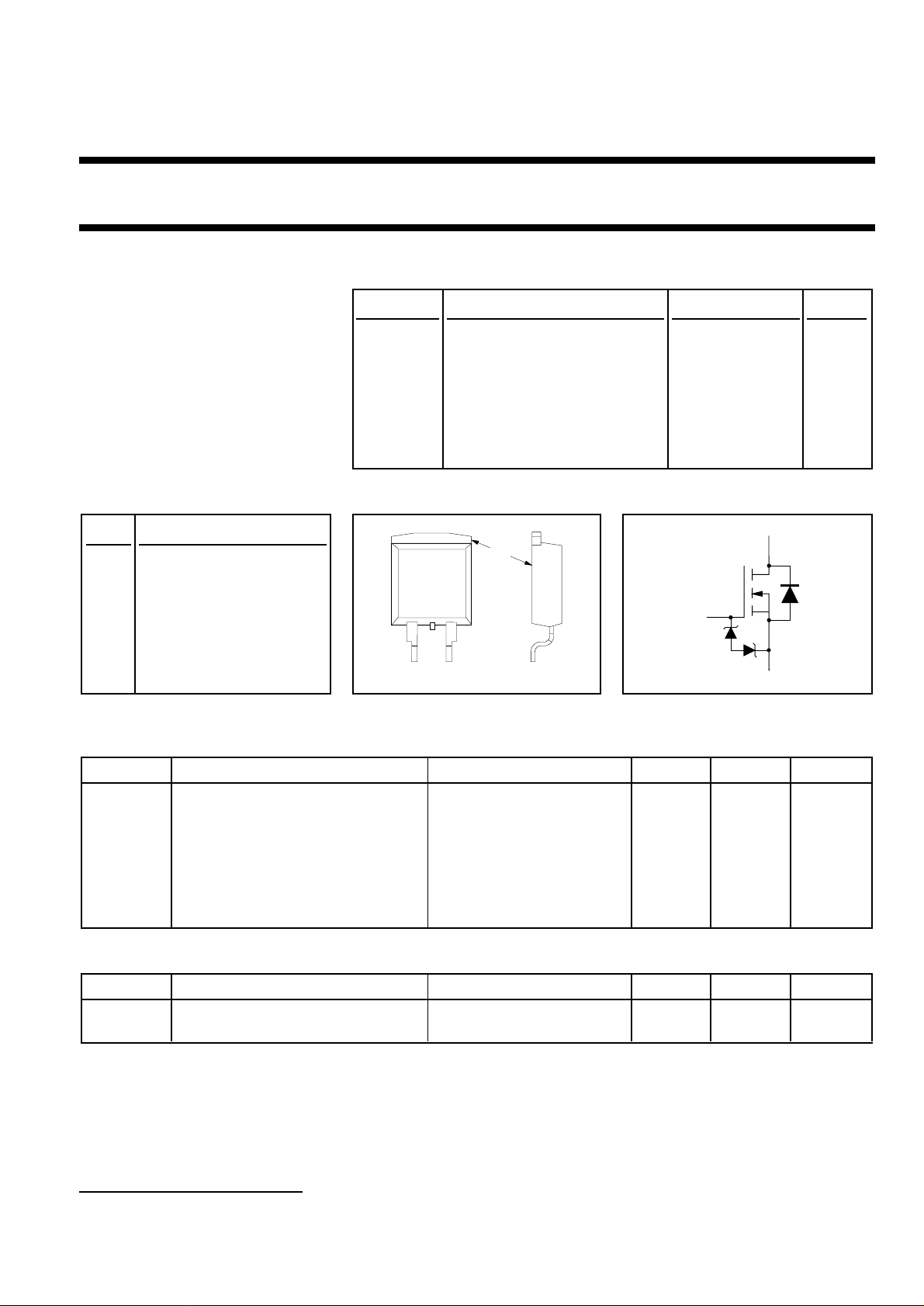
PINNING - SOT404 PIN CONFIGURATION SYMBOL
Drain-source voltage 55 V
Drain current (DC)
1
75 A
Total power dissipation 250 W
Junction temperature 175 ˚C
Drain-source on-state 8 mΩ
PIN DESCRIPTION
mb
d
1 gate
2 drain
3 source
mb drain
2
13
g
s
LIMITING VALUES
Limiting values in accordance with the Absolute Maximum System (IEC 134)
SYMBOL PARAMETER CONDITIONS MIN. MAX. UNIT
V
V
±V
I
D
I
D
I
DM
P
T
DS
DGR
tot
stg
GS
, T
j
Drain-source voltage - - 55 V
Drain-gate voltage RGS = 20 kΩ -55V
Gate-source voltage - - 10 V
Drain current (DC)
Drain current (DC)
1
1
Tmb = 25 ˚C - 75 A
Tmb = 100 ˚C - 75 A
Drain current (pulse peak value) Tmb = 25 ˚C - 240 A
Total power dissipation Tmb = 25 ˚C - 250 W
Storage & operating temperature - - 55 175 ˚C
ESD LIMITING VALUE
SYMBOL PARAMETER CONDITIONS MIN. MAX. UNIT
V
C
Electrostatic discharge capacitor Human body model - 2 kV
voltage (100 pF, 1.5 kΩ)
1 Current limited by package to 75A from a theoretical value of 125A.
December 1997 1 Rev 1.100
Philips Semiconductors Product specification
TrenchMOS transistor PHB125N06LT
Logic level FET
THERMAL RESISTANCES
SYMBOL PARAMETER CONDITIONS TYP. MAX. UNIT
R
th j-mb
R
th j-a
STATIC CHARACTERISTICS
Tj= 25˚C unless otherwise specified
SYMBOL PARAMETER CONDITIONS MIN. TYP. MAX. UNIT
V
(BR)DSS
V
GS(TO)
I
DSS
I
GSS
±V
(BR)GSS
R
DS(ON)
Thermal resistance junction to - - 0.6 K/W
mounting base
Thermal resistance junction to Minimum footprint,FR4 50 - K/W
ambient board
Drain-source breakdown VGS = 0 V; ID = 0.25 mA; 55 - - V
voltage Tj = -55˚C 50 - - V
Gate threshold voltage VDS = VGS; ID = 1 mA 1.0 1.5 2.0 V
Tj = 175˚C 0.5 - - V
Tj = -55˚C - - 2.3 V
Zero gate voltage drain current VDS = 55 V; VGS = 0 V; - 0.05 10 µA
Tj = 175˚C - - 500 uA
Gate source leakage current VGS = ±5 V; VDS = 0 V - 0.02 1 µA
Tj = 175˚C - - 10 µA
Gate-source breakdown IG = ±1 mA; 10 - - V
voltage
Drain-source on-state VGS = 5 V; ID = 25 A - 6.5 8 mΩ
resistance Tj = 175˚C - - 17 mΩ
DYNAMIC CHARACTERISTICS
Tmb = 25˚C unless otherwise specified
SYMBOL PARAMETER CONDITIONS MIN. TYP. MAX. UNIT
g
Q
Q
Q
C
C
C
t
t
t
t
L
L
fs
g(tot)
gs
gd
iss
oss
rss
d on
r
d off
f
d
s
Forward transconductance VDS = 25 V; ID = 25 A 40 90 - S
Total gate charge ID = 50 A; V
= 44 V; VGS = 5 V - 84 - nC
DD
Gate-source charge - 18 - nC
Gate-drain (Miller) charge - 39 - nC
Input capacitance VGS = 0 V; VDS = 25 V; f = 1 MHz - 5200 6900 pF
Output capacitance - 840 1000 pF
Feedback capacitance - 350 480 pF
Turn-on delay time VDD = 30 V; ID = 25 A; - 45 60 ns
Turn-on rise time VGS = 5 V; RG = 10 Ω - 120 170 ns
Turn-off delay time - 225 300 ns
Turn-off fall time - 100 135 ns
Internal drain inductance Measured from upper edge of drain - 3.5 - nH
tab to centre of die
Internal source inductance Measured from source lead - 7.5 - nH
soldering point to source bond pad
December 1997 2 Rev 1.100
Philips Semiconductors Product specification
TrenchMOS transistor PHB125N06LT
Logic level FET
REVERSE DIODE LIMITING VALUES AND CHARACTERISTICS
Tj = 25˚C unless otherwise specified
SYMBOL PARAMETER CONDITIONS MIN. TYP. MAX. UNIT
I
DR
I
DRM
V
SD
t
rr
Q
rr
AVALANCHE LIMITING VALUE
SYMBOL PARAMETER CONDITIONS MIN. TYP. MAX. UNIT
W
DSS
Continuous reverse drain - - 75 A
current
Pulsed reverse drain current - - 240 A
Diode forward voltage IF = 25 A; VGS = 0 V - 0.85 1.2 V
IF = 75 A; VGS = 0 V - 1.0 - V
Reverse recovery time IF = 75 A; -dIF/dt = 100 A/µs; - 65 - ns
Reverse recovery charge VGS = -10 V; VR = 30 V - 0.18 - µC
Drain-source non-repetitive ID = 75 A; VDD ≤ 25 V; - - 500 mJ
unclamped inductive turn-off VGS = 5 V; RGS = 50 Ω; Tmb = 25 ˚C
energy
December 1997 3 Rev 1.100
 Loading...