

Philips PHB11N03LT, PHD11N03LT Datasheet
Philips Semiconductors Product specification
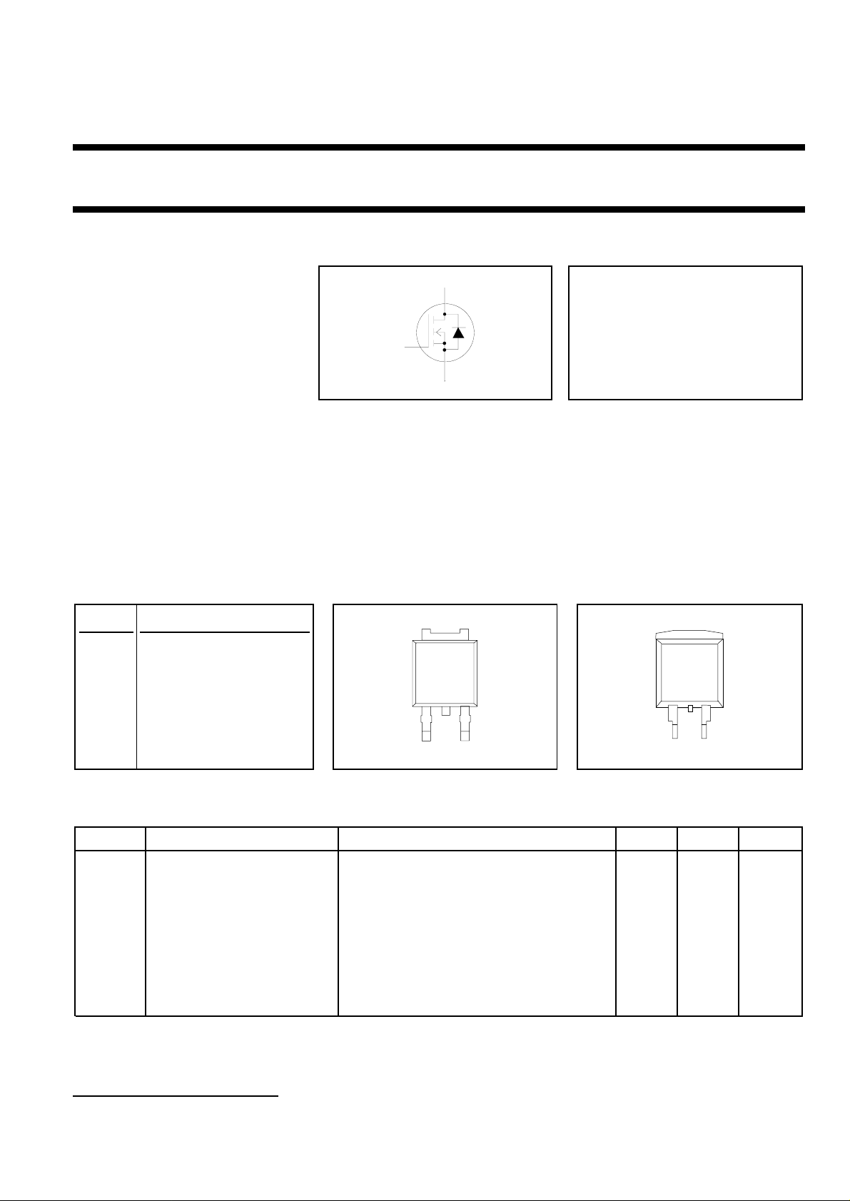
N-channel TrenchMOS transistor PHB11N03LT, PHD11N03LT
Logic level FET
FEATURES SYMBOL QUICK REFERENCE DATA
• ’Trench’ technology V
d
= 30 V
DSS
• Low on-state resistance
• Fast switching I
= 10.5 A
D
• Logic level compatible
g
R
R
s
≤ 150 mΩ (VGS = 5 V)
DS(ON)
≤ 130 mΩ (VGS = 10 V)
DS(ON)
GENERAL DESCRIPTION
N-channelenhancementmode,logic level, field-effect power transistor in a plastic envelopeusing’trench’technology.
Applications:-
• d.c. to d.c. converters
• switched mode power supplies
The PHB11N03LT is supplied in the SOT404 (D2PAK) surface mounting package.
The PHD11N03LT is supplied in the SOT428 (DPAK) surface mounting package.
PINNING SOT428 (DPAK) SOT404 (D2PAK)
PIN DESCRIPTION
1 gate
2 drain
1
tab
tab
3 source
tab drain
2
1
3
2
13
LIMITING VALUES
Limiting values in accordance with the Absolute Maximum System (IEC 134)
SYMBOL PARAMETER CONDITIONS MIN. MAX. UNIT
V
DSS
V
DGR
V
GS
V
GSM
I
D
I
DM
P
D
Tj, T
1 It is not possible to make contact to pin 2 of the SOT404 or SOT428 package
Drain-source voltage Tj = 25 ˚C to 175˚C - 30 V
Drain-gate voltage Tj = 25 ˚C to 175˚C; RGS = 20 kΩ -30V
Gate-source voltage - ± 15 V
Pulsed gate-source voltage - ± 20 V
Continuous drain current Tmb = 25 ˚C - 10.3 A
Tmb = 100 ˚C - 7.3 A
Pulsed drain current Tmb = 25 ˚C - 41 A
Total power dissipation Tmb = 25 ˚C - 33 W
Operating junction and - 55 175 ˚C
stg
storage temperature
September 1999 1 Rev 1.000

Philips Semiconductors Product specification
N-channel TrenchMOS transistor PHB11N03LT, PHD11N03LT
Logic level FET
AVALANCHE ENERGY LIMITING VALUES
Limiting values in accordance with the Absolute Maximum System (IEC 134)
SYMBOL PARAMETER CONDITIONS MIN. MAX. UNIT
E
AS
I
AS
THERMAL RESISTANCES
SYMBOL PARAMETER CONDITIONS TYP. MAX. UNIT
R
th j-mb
R
th j-a
Non-repetitive avalanche Unclamped inductive load, IAS = 3.3 A; - 25 mJ
energy tp = 220 µs; Tj prior to avalanche = 25˚C;
VDD ≤ 15 V; RGS = 50 Ω; VGS = 5 V; refer to
fig:15
Peak non-repetitive - 10.3 A
avalanche current
Thermal resistance junction - 4.5 K/W
to mounting base
Thermal resistance junction SOT428 and SOT404 package, pcb 50 - K/W
to ambient mounted, minimum footprint
ELECTRICAL CHARACTERISTICS
Tj= 25˚C unless otherwise specified
SYMBOL PARAMETER CONDITIONS MIN. TYP. MAX. UNIT
V
(BR)DSS
V
GS(TO)
R
DS(ON)
g
fs
I
GSS
I
DSS
Q
g(tot)
Q
gs
Q
gd
t
d on
t
r
t
d off
t
f
L
d
L
d
L
s
C
iss
C
oss
C
rss
Drain-source breakdown VGS = 0 V; ID = 0.25 mA; 30 - - V
voltage Tj = -55˚C 26 - - V
Gate threshold voltage VDS = VGS; ID = 1 mA 1.0 1.5 2.0 V
Tj = 175˚C 0.5 - - V
Tj = -55˚C - - 2.3 V
Drain-source on-state VGS = 10 V; ID = 5.5 A - 100 130 mΩ
resistance VGS = 5 V; ID = 5.5 A - 120 150 mΩ
Tj = 175˚C - 250 315 mΩ
Forward transconductance VDS = 25 V; ID = 5.5 A 4 7 - S
Gate source leakage current VGS = ±5 V; VDS = 0 V - 10 100 nA
Zero gate voltage drain VDS = 30 V; VGS = 0 V; - 0.05 10 µA
current Tj = 175˚C - - 500 µA
Total gate charge ID = 10 A; V
= 15 V; VGS = 5 V - 3.8 - nC
DD
Gate-source charge - 1.2 - nC
Gate-drain (Miller) charge - 1.7 - nC
Turn-on delay time VDD = 30 V; RD = 2.7 Ω;-616ns
Turn-on rise time RG = 10 Ω; VGS = 5 V - 64 80 ns
Turn-off delay time Resistive load - 20 30 ns
Turn-off fall time - 26 40 ns
Internal drain inductance Measured from tab to centre of die - 3.5 - nH
Internal drain inductance Measured from drain lead to centre of die - 4.5 - nH
(SOT78 package only)
Internal source inductance Measured from source lead to source - 7.5 - nH
bond pad
Input capacitance VGS = 0 V; VDS = 25 V; f = 1 MHz - 250 330 pF
Output capacitance - 55 75 pF
Feedback capacitance - 42 55 pF
September 1999 2 Rev 1.000

Philips Semiconductors Product specification
N-channel TrenchMOS transistor PHB11N03LT, PHD11N03LT
Logic level FET
REVERSE DIODE LIMITING VALUES AND CHARACTERISTICS
Tj = 25˚C unless otherwise specified
SYMBOL PARAMETER CONDITIONS MIN. TYP. MAX. UNIT
I
S
I
SM
V
SD
t
rr
Q
rr
Continuous source current - - 10.3 A
(body diode)
Pulsed source current (body - - 41 A
diode)
Diode forward voltage IF = 10 A; VGS = 0 V - 1.15 1.5 V
Reverse recovery time IF = 10 A; -dIF/dt = 100 A/µs; - 35 - ns
Reverse recovery charge VGS = 0 V; VR = 30 V - 55 - nC
September 1999 3 Rev 1.000
Philips Semiconductors Product specification
N-channel TrenchMOS transistor PHB11N03LT, PHD11N03LT
Logic level FET
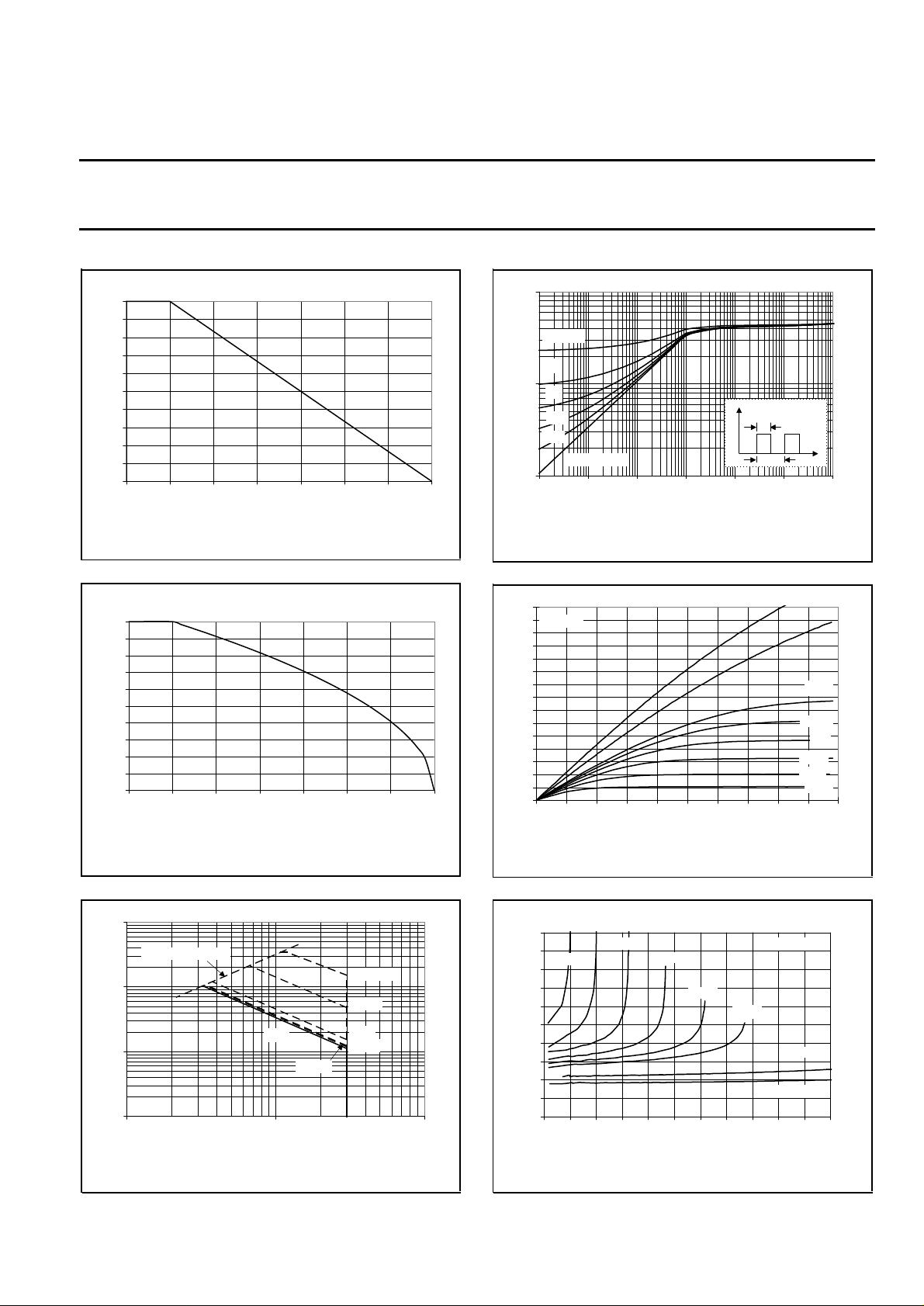
Normalised Power Derating, PD (%)
100
90
80
70
60
50
40
30
20
10
0
0 25 50 75 100 125 150 175
Mounting Base temperature, Tmb (C)
Fig.1. Normalised power dissipation.
PD% = 100⋅PD/P
Normalised Current Derating, ID (%)
100
90
80
70
60
50
40
30
20
10
0
0 25 50 75 100 125 150 175
Mounting Base temperature, Tmb (C)
D 25 ˚C
= f(Tmb)
Fig.2. Normalised continuous drain current.
ID% = 100⋅ID/I
= f(Tmb); conditions: VGS ≥ 5 V
D 25 ˚C
Transient thermal impedance, Zth j-mb (K/W)
10
D = 0.5
0.2
1
0.1
P
0.05
0.02
single pulse
0.1
1E-06 1E-05 1E-04 1E-03 1E-02 1E-01 1E+00
Pulse width, tp (s)
D
tp
D = tp/T
T
Fig.4. Transient thermal impedance.
Z
= f(t); parameter D = tp/T
th j-mb
Drain Current, ID (A)
15
14
Tj = 25 C VGS = 10V
13
12
11
10
9
8
7
6
5
4
3
2
1
0
0 0.2 0.4 0.6 0.8 1 1.2 1.4 1.6 1.8 2
Drain-Source Voltage, VDS (V)
5 V
3.4 V
3.2 V
3 V
2.8 V
2.6 V
2.4 V
Fig.5. Typical output characteristics, Tj = 25 ˚C
ID = f(VDS)
.
Peak Pulsed Drain Current, IDM (A)
100
RDS(on) = VDS/ ID
10
D.C.
1
0.1
1 10 100
Drain-Source Voltage, VDS (V)
100 ms
tp = 10 us
100 us
1 ms
10 ms
Fig.3. Safe operating area. Tmb = 25 ˚C
ID & IDM = f(VDS); IDM single pulse; parameter t
p
Drain-Source On Resistance, RDS(on) (Ohms)
0.5
0.45
2.4 V
0.4
0.35
0.3
0.25
0.2
0.15
0.1
0.05
0
01234567891011
2.6 V
2.8V
3 V
Drain Current, ID (A)
Tj = 25 C
3.2 V
3.4 V
5 V
VGS = 10V
Fig.6. Typical on-state resistance, Tj = 25 ˚C
R
= f(ID)
DS(ON)
.
September 1999 4 Rev 1.000
 Loading...