

查询PESD12VS2UT供应商
DISCRETE SEMICONDUCTORS
DATA SH EET
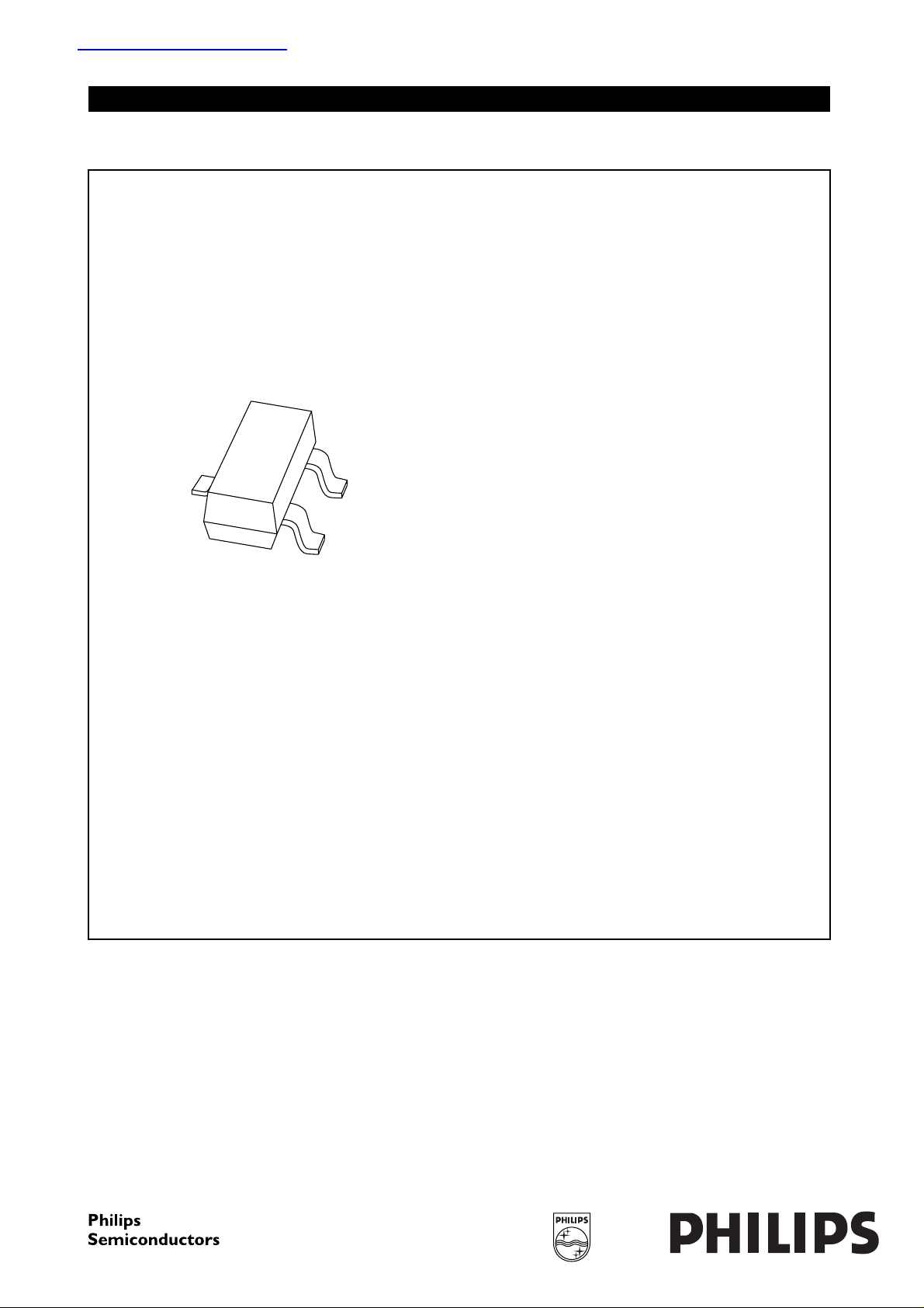
PESDxS2UT series
Double ESD protection diodes in
SOT23 package
Product specification
Supersedes data of 2003 Aug 20
2004 Apr 15
Philips Semiconductors Product specification
Double ESD protection diodes
in SOT23 package
FEATURES
• Uni-directional ESD protection of up to two lines
• Max. peak pulse power: Ppp= 330 W at tp= 8/20 µs
• Low clamping voltage: V
• Ultra-low reverse leakage current: IRM< 700 nA
• ESD protection > 23 kV
• IEC 61000-4-2; level 4 (ESD)
• IEC 61000-4-5 (surge); Ipp= 18 A at tp= 8/20 µs.
APPLICATIONS
• Computers and peripherals
• Communication systems
• Audio and video equipment
• High speed data lines
• Parallel ports.
= 20 V at Ipp=18A
(CL)R
PESDxS2UT series
QUICK REFERENCE DATA
SYMBOL PARAMETER VALUE UNIT
V
RWM
C
d
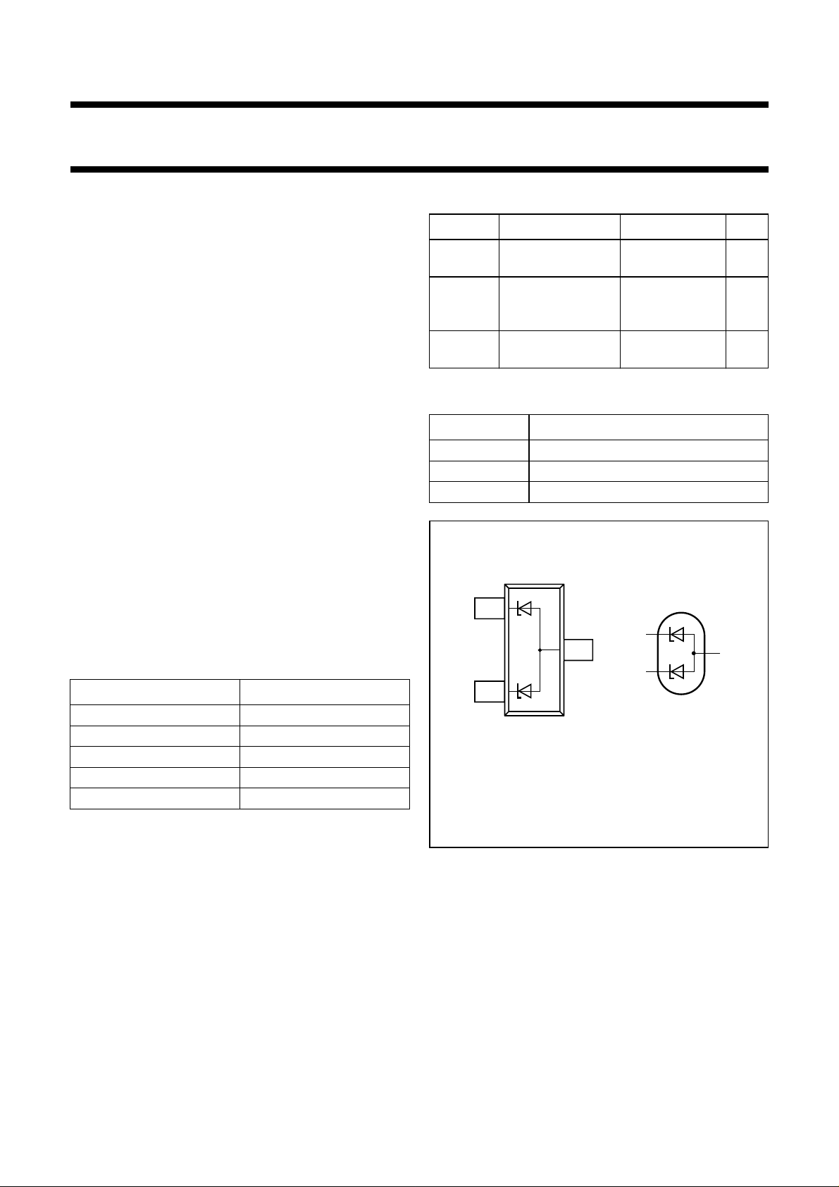
PINNING
reverse stand-off
voltage
diode capacitance
VR=0V;
3.3, 5.2, 12, 15
and 24
207,152,38,32
and 23
f = 1 MHz
number of
2
protected lines
PIN DESCRIPTION
1 cathode 1
2 cathode 2
3 common anode
V
pF
DESCRIPTION
Uni-directional double ESD protection diodes in a SOT23
plastic package. Designed to protect up to two
transmission or data lines from ElectroStatic Discharge
(ESD) damage.
MARKING
TYPE NUMBER MARKING CODE
(1)
PESD3V3S2UT *U9
PESD5V2S2UT *U1
PESD12VS2UT *U2
PESD15VS2UT *U3
PESD24VS2UT *U4
Note
1. * = p : made in Hong Kong.
* = t : made in Malaysia.
* = W : made in China.
1
3
2
001aaa490
1
2
sym022
Fig.1 Simplified outline (SOT23) and symbol.
3
2004 Apr 15 2

Philips Semiconductors Product specification
Double ESD protection diodes
PESDxS2UT series
in SOT23 package
ORDERING INFORMATION
TYPE NUMBER
PESD3V3S2UT − plastic surface mounted package; 3 leads SOT23
PESD5V2S2UT
PESD12VS2UT
PESD15VS2UT
PESD24VS2UT
LIMITING VALUES
In accordance with the Absolute Maximum Rating System (IEC 60134).
SYMBOL PARAMETER CONDITIONS MIN. MAX. UNIT
P
pp
I
pp
T
j
T
amb
T
stg
peak pulse power 8/20 µs pulse; notes 1 and 2
PESD3V3S2UT − 330 W
PESD5V2S2UT − 260 W
PESD12VS2UT − 180 W
PESD15VS2UT − 160 W
PESD24VS2UT − 160 W
peak pulse current 8/20 µs pulse; notes 1 and 2
PESD3V3S2UT − 18 A
PESD5V2S2UT − 15 A
PESD12VS2UT − 5A
PESD15VS2UT − 5A
PESD24VS2UT − 3A
junction temperature − 150 °C
operating ambient temperature −65 +150 °C
storage temperature −65 +150 °C
NAME DESCRIPTION VERSION
PACKAGE
Notes
1. Non-repetitive current pulse 8/20 µs exponential decay waveform; see Fig.2.
2. Measured across either pins 1 and 3 or pins 2 and 3.
2004 Apr 15 3
Philips Semiconductors Product specification
Double ESD protection diodes
PESDxS2UT series
in SOT23 package
ESD maximum ratings
SYMBOL PARAMETER CONDITIONS VALUE UNIT
ESD electrostatic discharge
capability
Notes
1. Device stressed with ten non-repetitive ElectroStatic Discharge (ESD) pulses; see Fig.3.
2. Measured across either pins 1 and 3 or pins 2 and 3.
ESD standards compliance
IEC 61000-4-2 (contact discharge);
notes 1 and 2
PESD3V3S2UT 30 kV
PESD5V2S2UT 30 kV
PESD12VS2UT 30 kV
PESD15VS2UT 30 kV
PESD24VS2UT 23 kV
HBM MIL-Std 883
PESDxS2UT series 10 kV
ESD STANDARD CONDITIONS
IEC 61000-4-2; level 4 (ESD); see Fig.3 >15 kV (air); > 8 kV (contact)
HBM MIL-Std 883; class 3 >4 kV
120
handbook, halfpage
I
pp
(%)
80
40
0
010
100 % Ipp; 8 µs
−t
e
20
MLE218
50 % Ipp; 20 µs
30
t (µs)
40
100 %
90 %
10 %
I
pp
tr = 0.7 to 1 ns
30 ns
001aaa191
t
60 ns
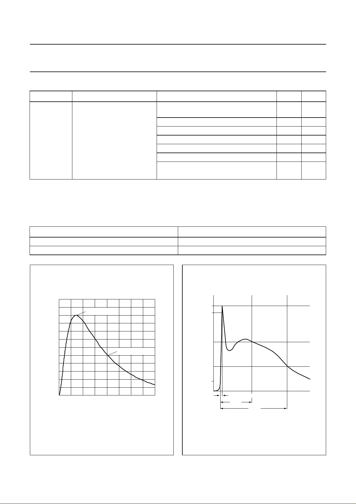
Fig.2 8/20 µs pulse waveform according to
IEC 61000-4-5.
2004 Apr 15 4
Fig.3 ElectroStatic Discharge (ESD) pulse
waveform according to IEC 61000-4-2.

Philips Semiconductors Product specification
Double ESD protection diodes
PESDxS2UT series
in SOT23 package
ELECTRICAL CHARACTERISTICS
Tj=25°C unless otherwise specified.
SYMBOL PARAMETER CONDITIONS MIN. TYP. MAX. UNIT
V
I
V
C
V
RM
RWM
BR
d
(CL)R
reverse stand-off voltage
PESD3V3S2UT −−3.3 V
PESD5V2S2UT −−5.2 V
PESD12VS2UT −−12 V
PESD15VS2UT −−15 V
PESD24VS2UT −−24 V
reverse leakage current
PESD3V3S2UT V
PESD5V2S2UT V
PESD12VS2UT V
PESD15VS2UT V
PESD24VS2UT V
= 3.3 V − 0.7 2 µA
RWM
= 5.2 V − 0.15 1 µA
RWM
= 12 V − <0.02 1 µA
RWM
= 15 V − <0.02 1 µA
RWM
= 24 V − <0.02 1 µA
RWM
breakdown voltage IZ = 5 mA
PESD3V3S2UT 5.2 5.6 6.0 V
PESD5V2S2UT 6.4 6.8 7.2 V
PESD12VS2UT 14.7 15.0 15.3 V
PESD15VS2UT 17.6 18.0 18.4 V
PESD24VS2UT 26.5 27.0 27.5 V
diode capacitance f = 1 MHz; VR=0V
PESD3V3S2UT − 207 300 pF
PESD5V2S2UT − 152 200 pF
PESD12VS2UT − 38 75 pF
PESD15VS2UT − 32 70 pF
PESD24VS2UT − 23 50 pF
clamping voltage notes 1 and 2
PESD3V3S2UT Ipp=1A −−7V
Ipp=18A −−20 V
PESD5V2S2UT Ipp=1A −−9V
Ipp=15A −−20 V
PESD12VS2UT Ipp=1A −−19 V
Ipp=5A −−35 V
PESD15VS2UT Ipp=1A −−23 V
Ipp=5A −−40 V
PESD24VS2UT Ipp=1A −−36 V
Ipp=3A −−70 V
2004 Apr 15 5

Philips Semiconductors Product specification
Double ESD protection diodes
PESDxS2UT series
in SOT23 package
SYMBOL PARAMETER CONDITIONS MIN. TYP. MAX. UNIT
R
diff
Notes
1. Non-repetitive current pulse 8/20 µs exponential decay waveform; see Fig.2.
2. Measured either across pins 1 and 3 or pins 2 and 3.
GRAPHICAL DATA
4
10
differential resistance
PESD3V3S2UT IR=1mA −−400 Ω
PESD5V2S2UT IR=1mA −−80 Ω
PESD12VS2UT IR=1mA −−200 Ω
PESD15VS2UT IR=1mA −−225 Ω
PESD24VS2UT IR= 0.5 mA −−300 Ω
001aaa147
1.2
001aaa193
P
pp
(W)
3
10
2
10
10
110
(1) PESD3V3S2UT and PESD5V2S2UT.
(2) PESD12VS2UT, PESD15VS2UT, PESD24VS2UT
T
=25°C.
amb
tp= 8/20 µs exponential decay waveform; see Fig.2.
10 10
(1)
(2)
2
3
10
t
p
4
(µs)
P
P
pp(25˚C)
pp
0.8
0.4
Fig.5 Relative variation of peak pulse power as a
Fig.4 Peak pulse power dissipation as a function
of pulse time; typical values.
0
0 20015050 100
Tj (°C)
function of junction temperature; typical
values.
2004 Apr 15 6

Philips Semiconductors Product specification
Double ESD protection diodes
in SOT23 package
240
C
d
(pF)
200
160
120
80
40
054231
(1) PESD3V3S2UT; V
(2) PESD5V2S2UT; V
T
= 25 °C; f = 1 MHz.
amb
(1)
(2)
RWM
RWM
= 3.3 V.
=5V.
001aaa148
VR (V)
50
C
d
(pF)
40
30
20
10
0
0252010 155
(1) PESD12VS2UT; V
(2) PESD15VS2UT; V
(3) PESD24VS2UT; V
T
= 25 °C; f = 1 MHz.
amb
PESDxS2UT series
001aaa149
(1)
(2)
(3)
=12V.
RWM
=15V.
RWM
=24V.
RWM
VR (V)
Fig.6 Diode capacitance as a function of reverse
voltage; typical values.
Fig.7 Diode capacitance as a function of reverse
voltage; typical values.
2004 Apr 15 7

Philips Semiconductors Product specification
Double ESD protection diodes
in SOT23 package
10
I
R
I
R(25˚C)
1
−1
10
−100 150100050−50
(1) PESD3V3S2UT; V
PESD5V2S2UT; V
RWM
RWM
(1)
= 3.3 V.
=5V.
001aaa270
Tj (°C)
PESDxS2UT series
IR is less than 10 nA at 150 °C for:
PESD12V52UT; V
PESD15VS2UT; V
PESD24VS2UT; V
RWM
RWM
RWM
=12V.
=15V.
=24V.
Fig.8 Relative variation of reverse leakage
current as a function of junction
temperature; typical values.
2004 Apr 15 8

Philips Semiconductors Product specification
Double ESD protection diodes
in SOT23 package
ESD TESTER
R
Z
C
Z
note 1
Note 1: IEC61000-4-2 network
C
= 150 pF; RZ = 330 Ω
Z
vertical scale = 200 V/div
horizontal scale = 50 ns/div
D.U.T.: PESDxS2UT
450 Ω
RG 223/U
50 Ω coax
GND
10×
ATTENUATOR
PESDxS2UT series
4 GHz DIGITAL
OSCILLOSCOPE
50 Ω
vertical scale = 20 V/div
horizontal scale = 50 ns/div
PESD24VS2UT
GND
unclamped +1 kV ESD voltage waveform
(IEC61000-4-2 network)
GND
vertical scale = 200 V/div
horizontal scale = 50 ns/div
unclamped −1 kV ESD voltage waveform
(IEC61000-4-2 network)
GND
GND
GND
GND
clamped +1 kV ESD voltage waveform
(IEC61000-4-2 network)
GND
clamped −1 kV ESD voltage waveform
(IEC61000-4-2 network)
PESD15VS2UT
PESD12VS2UT
PESD5V2S2UT
PESD3V3S2UT
vertical scale = 10 V/div
horizontal scale = 50 ns/div
001aaa492
Fig.9 ESD clamping test set-up and waveforms.
2004 Apr 15 9

Philips Semiconductors Product specification
Double ESD protection diodes
PESDxS2UT series
in SOT23 package
APPLICATION INFORMATION
The PESDxS2UT series is designed for uni-directional protection for up to two lines against damage caused by
ElectroStatic Discharge (ESD) and surge pulses. The PESDxS2UT series may be used on lines where the signal
polarities are below ground. PESDxS2UT series provide a surge capability of up to 330 W (Ppp) per line for an 8/20 µs
waveform.
line 1 to be protected
line 2 to be protected
PESDxS2UT
ground
unidirectional protection
of two lines
bidirectional protection
Fig.10 Typical application: ESD protection of data lines.
line 1 to be protected
PESDxS2UT
ground
of one line
001aaa491
Circuit board layout and protection device placement
Circuit board layout is critical for the suppression of ESD, Electrical Fast Transient (EFT) and surge transients. The
following guidelines are recommended:
• Place the PESDxS2UT as close as possible to the input terminal or connector.
• The path length between the PESDxS2UT and the protected line should be minimized.
• Keep parallel signal paths to a minimum.
• Avoid running protected conductors in parallel with unprotected conductors.
• Minimize all printed-circuit board conductive loops including power and ground loops.
• Minimize the length of transient return paths to ground.
• Avoid using shared return paths to a common ground point.
• Ground planes should be used whenever possible. For multilayer printed-circuit boards use ground vias.
2004 Apr 15 10

Philips Semiconductors Product specification
Double ESD protection diodes
PESDxS2UT series
in SOT23 package
PACKAGE OUTLINE
Plastic surface mounted package; 3 leads SOT23
D
3
E
H
E
AB
X
v
M
A
12
e
1
DIMENSIONS (mm are the original dimensions)
A
1
0.1
b
p
0.48
0.15
0.38
0.09
IEC JEDEC EIAJ
UNIT
A
max.
1.1
mm
0.9
OUTLINE
VERSION
SOT23 TO-236AB
b
p
e
cD
3.0
2.8
w
M
B
0 1 2 mm
scale
e
0.95
H
1
2.5
2.1
E
1.4
1.9
1.2
REFERENCES
e
Q
A
A
1
c
L
p
detail X
L
Qwv
p
E
0.55
0.45
0.15
0.45
0.2
0.1
EUROPEAN
PROJECTION
ISSUE DATE
97-02-28
99-09-13
2004 Apr 15 11

Philips Semiconductors Product specification
Double ESD protection diodes
PESDxS2UT series
in SOT23 package
DATA SHEET STATUS
LEVEL
I Objective data Development This data sheet contains data from the objective specification for product
II Preliminary data Qualification This data sheet contains data from the preliminary specification.
III Product data Production This data sheet contains data from the product specification. Philips
Notes
1. Please consult the most recently issued data sheet before initiating or completing a design.
2. The product status of the device(s) described in this data sheet may have changed since this data sheet was
published. The latest information is available on the Internet at URL http://www.semiconductors.philips.com.
3. For data sheets describing multiple type numbers, the highest-level product status determines the data sheet status.
DATA SHEET
STATUS
(1)
PRODUCT
STATUS
(2)(3)
development. Philips Semiconductors reserves the right to change the
specification in any manner without notice.
Supplementary data will be published at a later date. Philips
Semiconductors reserves the right to change the specification without
notice, in order to improve the design and supply the best possible
product.
Semiconductors reserves the right to make changes at any time in order
to improve the design, manufacturing and supply. Relevant changes will
be communicated via a Customer Product/Process Change Notification
(CPCN).
DEFINITION
DEFINITIONS
Short-form specification The data in a short-form
specification is extracted from a full data sheet with the
same type number and title. For detailed information see
the relevant data sheet or data handbook.
Limiting values definition Limiting values given are in
accordance with the Absolute Maximum Rating System
(IEC 60134). Stress above one or more of the limiting
values may cause permanent damage to the device.
These are stress ratings only and operation of the device
attheseoratany other conditions above those given in the
Characteristics sections of the specification is not implied.
Exposure to limiting values for extended periods may
affect device reliability.
Application information Applications that are
described herein for any of these products are for
illustrative purposes only. Philips Semiconductors make
norepresentationorwarrantythatsuchapplicationswillbe
suitable for the specified use without further testing or
modification.
DISCLAIMERS
Life support applications These products are not
designed for use in life support appliances, devices, or
systems where malfunction of these products can
reasonably be expected to result in personal injury. Philips
Semiconductorscustomersusingorsellingtheseproducts
for use in such applications do so at their own risk and
agree to fully indemnify Philips Semiconductors for any
damages resulting from such application.
Right to make changes Philips Semiconductors
reserves the right to make changes in the products including circuits, standard cells, and/or software described or contained herein in order to improve design
and/or performance. When the product is in full production
(status ‘Production’), relevant changes will be
communicated via a Customer Product/Process Change
Notification (CPCN). Philips Semiconductors assumes no
responsibility or liability for the use of any of these
products, conveys no license or title under any patent,
copyright, or mask work right to these products, and
makes no representations or warranties that these
products are free from patent, copyright, or mask work
right infringement, unless otherwise specified.
2004 Apr 15 12

Philips Semiconductors – a w orldwide compan y
Contact information
For additional information please visit http://www.semiconductors.philips.com. Fax: +31 40 27 24825
For sales offices addresses send e-mail to: sales.addresses@www.semiconductors.philips.com.
© Koninklijke Philips Electronics N.V. 2004
All rights are reserved. Reproduction in whole or in part is prohibited without the prior written consent of the copyright owner.
The information presented in this document does not form part of any quotation or contract, is believed to be accurate and reliable and may be changed
without notice. No liability will be accepted by the publisher for any consequence of its use. Publication thereof does not convey nor imply any license
under patent- or other industrial or intellectual property rights.
Printed in The Netherlands R76/03/pp13 Date of release: 2004 Apr 15 Document order number: 9397 750 12823
SCA76
 Loading...