

7
查询PESD3V3L4UG供应商
DISCRETE SEMICONDUCTORS
DATA SH EET
e
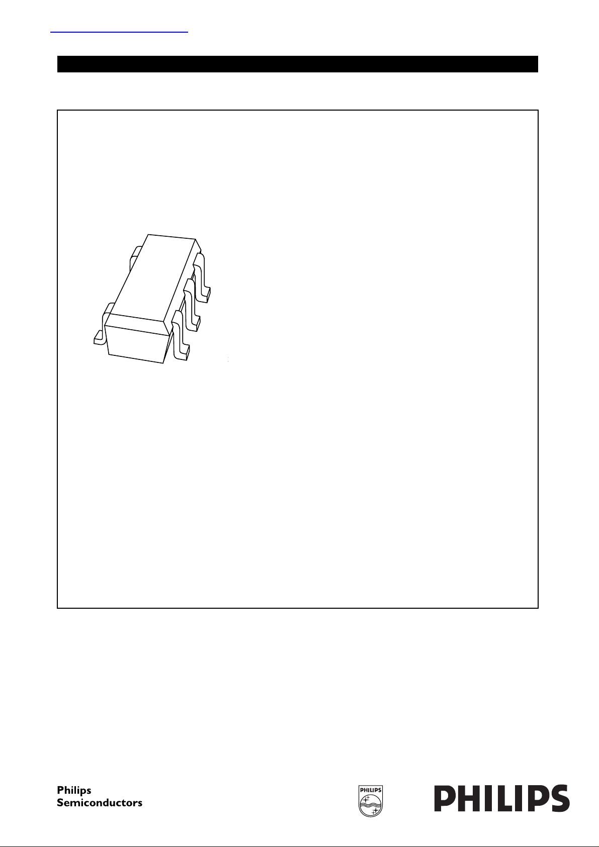
MBD12
PESDxL4UG series
Low capacitance quadruple ESD
protection diode array in SOT353
package
Product specification 2004 Mar 23
Philips Semiconductors Product specification
Low capacitance quadruple ESD
protection diode array in SOT353 package
FEATURES
• Uni-directional ESD protection of up to four lines
• Low diode capacitance
• Maximum peak pulse power: Ppp= 30 W at tp= 8/20µs
• Low clamping voltage: V
• Ultra low leakage current: IRM= 5 nA at V
= 12 V at Ipp=3A
CL(R)
RWM
=5V
• ESD protection > 20 kV
• IEC 61000-4-2; level 4 (ESD).
APPLICATIONS
• Cellular handsets and accessories
• Portable electronics
• Computers and peripherals
• Communications systems
• Audio and video equipment.
DESCRIPTION
ESD protectiondiode arrays designed to protect up to four
transmissions or data lines from ElectroStatic Discharge
(ESD) damage and other transients.
QUICK REFERENCE DATA
SYMBOL PARAMETER VALUE UNIT
V
C
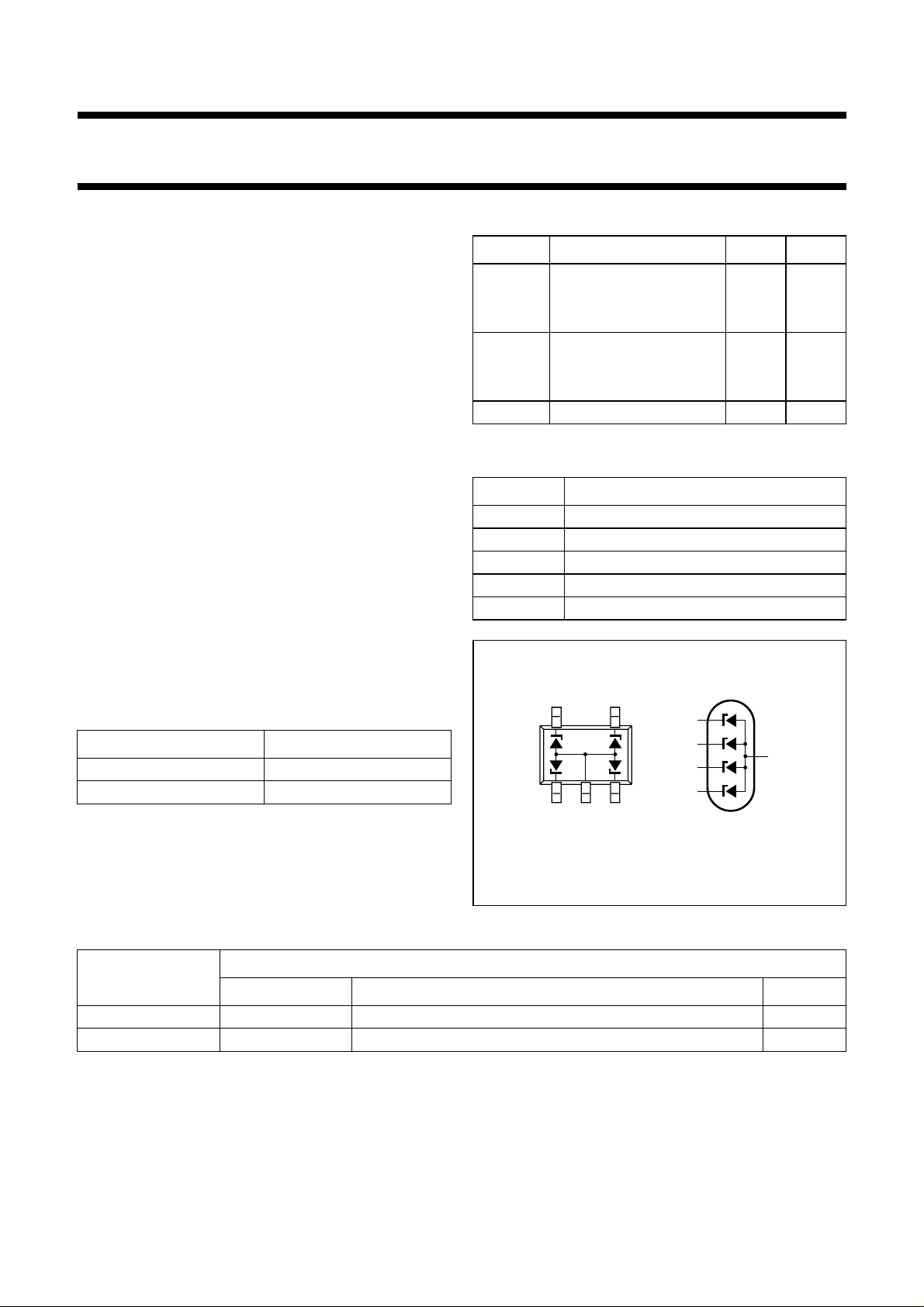
PINNING
PESDxL4UG series
RWM
d
PIN DESCRIPTION
reverse standoff voltage
PESD3V3L4UG 3.3 V
PESD5V0L4UG 5 V
diode capacitance
PESD3V3L4UG 22 pF
PESD5V0L4UG 16 pF
number of protected lines 4
1 cathode 1
2 common anode
3 cathode 2
4 cathode 3
5 cathode 4
MARKING
TYPE NUMBER MARKING
PESD3V3L4UG L1
PESD5V0L4UG L2
handbook, halfpage
5
4
1
3
4
5
31
2
2
MGT580
Fig.1 Simplified outline (SOT353) and symbol.
ORDERING INFORMATION
PACKAGE
TYPE NUMBER
NAME DESCRIPTION VERSION
PESD3V3L4UG − plastic surface mounted package; 5 leads SOT353
PESD5V0L4UG − plastic surface mounted package; 5 leads SOT353
2004 Mar 23 2
Philips Semiconductors Product specification
Low capacitance quadruple ESD
PESDxL4UG series
protection diode array in SOT353 package
LIMITING VALUES
In accordance with the Absolute Maximum Rating System (IEC 60134).
SYMBOL PARAMETER CONDITIONS MIN. MAX. UNIT
Per diode
I
pp
P
I
FSM
I
ZSM
P
P
T
T
T
pp
tot
ZSM
stg
j
amb
peak pulse current 8/20 µs; notes 1 and 2
PESD3V3L4UG − 3A
PESD5V0L4UG − 2.5 A
peak pulse power 8/20 µs; notes 1 and 2 − 30 W
non-repetitive peak forward
tp= 1 ms; square pulse − 3.5 A
current
non-repetitive peak reverse
tp= 1 ms; square pulse
current
PESD3V3L4UG − 0.9 A
PESD5V0L4UG − 0.8 A
total power dissipation T
non-repetitivepeak reversepower
=25°C; note 3 − 300 mW
amb
tp= 1 ms; square pulse; see Fig.4 − 6W
dissipation
storage temperature −65 +150 °C
junction temperature − 150 °C
operating ambient temperature −65 +150 °C
Notes
1. Non-repetitive current pulse 8/20 µs exponentially decaying waveform; see Fig.5.
2. Between any of pins 1, 3, 4 or 5 and pin 2.
3. Device mounted on standard printed-circuit board.
ESD maximum ratings
SYMBOL PARAMETER CONDITIONS VALUE UNIT
Per diode
ESD electrostatic discharge capability IEC 61000-4-2 (contact
20 kV
discharge); notes 1 and 2
HBM MIL-Std 883 10 kV
Notes
1. Device stressed with ten non-repetitive Electrostatic Discharge (ESD) pulses.
2. Measured from any of pins 1, 3, 4, or 5 to pin 2.
ESD standards compliance
STANDARD CONDITION
IEC 61000-4-2, level 4 (ESD) >15 kV (air); >8 kV (contact)
HBM MIL-Std 883, class 3 >4 kV
2004 Mar 23 3

Philips Semiconductors Product specification
Low capacitance quadruple ESD
PESDxL4UG series
protection diode array in SOT353 package
THERMAL CHARACTERISTICS
SYMBOL PARAMETER CONDITIONS VALUE UNIT
R
th(j-a)
R
th(j-s)
Note
1. Solder point of common anode (pin 2).
ELECTRICAL CHARACTERISTICS
Tj=25°C unless otherwise specified.
SYMBOL PARAMETER CONDITIONS MIN. TYP. MAX. UNIT
Per diode
V
F
I
RM
V
CL(R)
V
RWM
V
BR
r
diff
C
d
thermal resistance from junction to ambient all diodes loaded 410 K/W
thermal resistance from junction to solder point one diode loaded; note 1 200 K/W
all diodes loaded; note 1 185 K/W
forward voltage IF= 200 mA − 1 1.2 V
reverse leakage current
PESD3V3L4UG V
PESD5V0L4UG V
= 3.3 V − 75 300 nA
RWM
=5V − 525nA
RWM
clamping voltage
PESD3V3L4UG Ipp= 1 A; notes 1 and 2 −−8V
Ipp= 3 A; notes 1 and 2 −−12 V
PESD5V0L4UG Ipp= 1 A; notes 1 and 2 −−10 V
Ipp= 2.5 A; notes 1 and 2 −−13 V
reverse stand-off voltage
PESD3V3L4UG −−3.3 V
PESD5V0L4UG −−5V
breakdown voltage IZ=1mA
PESD3V3L4UG 5.32 5.6 5.88 V
PESD5V0L4UG 6.46 6.8 7.14 V
differential resistance IR=1mA
PESD3V3L4UG −−200 Ω
PESD5V0L4UG −−100 Ω
diode capacitance
PESD3V3L4UG VR= 0 V; f = 1 MHz − 22 28 pF
VR= 5 V; f = 1 MHz − 12 17 pF
PESD5V0L4UG VR= 0 V; f = 1 MHz − 16 19 pF
VR= 5 V; f = 1 MHz − 811pF
Notes
1. Non-repetitive current pulse 8 × 20 ms exponentially decay waveform; see Fig.5.
2. Between any of pins 1, 3, 4 or 5 and pin 2.
2004 Mar 23 4
Philips Semiconductors Product specification
Low capacitance quadruple ESD
protection diode array in SOT353 package
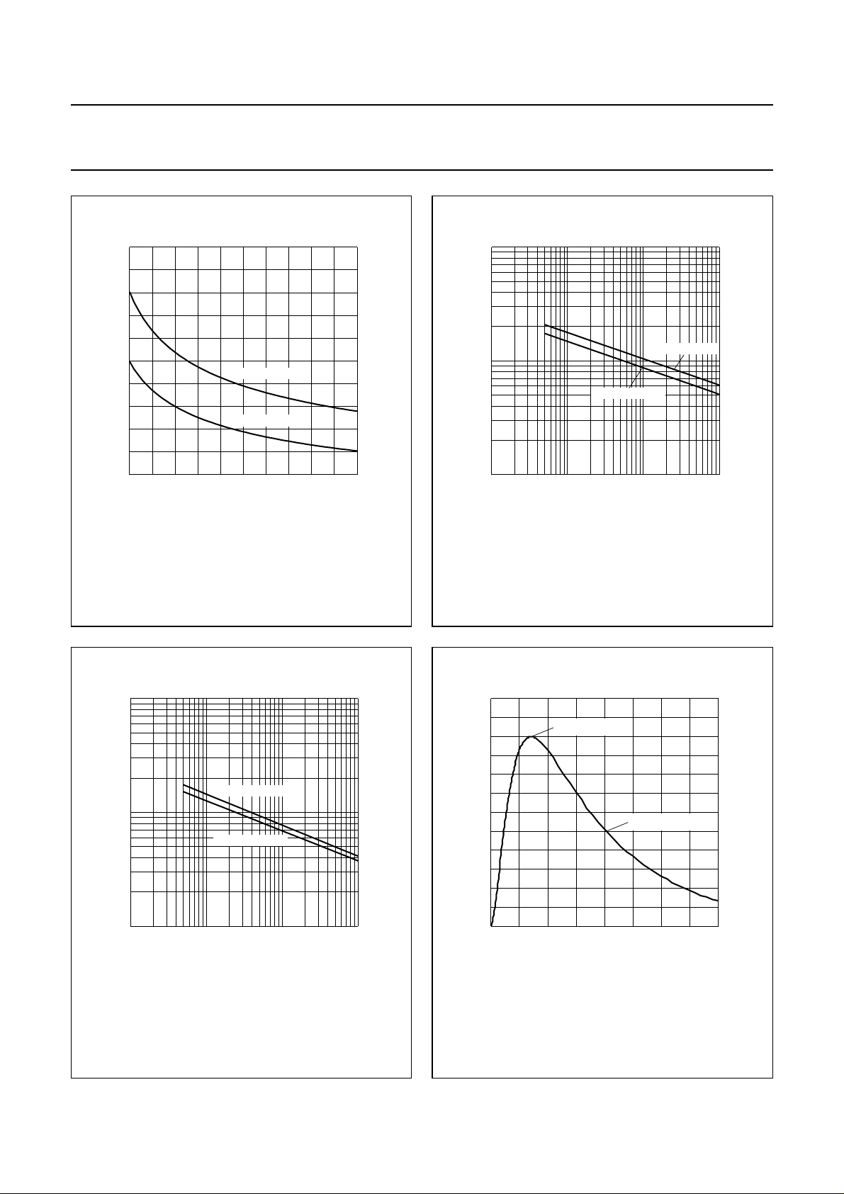
26
handbook, halfpage
C
d
(pF)
22
18
14
10
6
05
PESD3V3L4UG
PESD5V0L4UG
1234
MCE657
VR (V)
10
handbook, halfpage
I
ZSM
(A)
1
−1
10
−2
10
PESDxL4UG series
MCE658
PESD3V3L4UG
PESD5V0L4UG
−1
10
1
tp (ms)
10
Fig.2 Diode capacitance as a function of reverse
voltage; typical values.
2
10
handbook, halfpage
P
ZSM
(W)
10
1
−2
10
PESD3V3L4UG
PESD5V0L4UG
−1
10
1
MCE659
tp (ms)
Fig.3 Maximum non-repetitive peak reverse
current as a function of pulse time.
120
handbook, halfpage
I
pp
(%)
80
40
10
0
010
100 % Ipp; 8 µs
−t
e
20
50 % Ipp; 20 µs
MLE218
t (µs)
40
30
Fig.4 Maximum non-repetitive peak reverse
power dissipation as a function of pulse
duration (square pulse).
2004 Mar 23 5
Fig.5 8/20 µs pulse waveform according to
IEC 61000-4-5.

Philips Semiconductors Product specification
Low capacitance quadruple ESD
protection diode array in SOT353 package
ESD TESTER DIGITIZING
R
Z
C
Z
IEC 61000-4-2 network
= 150 pF; RZ = 330 Ω
C
Z
450 Ω
D.U.T.: PESDxL4UG
vertical scale = 200 V/div
horizontal scale = 50 ns/div
RG 223/U
50 Ω coax
GND2
PESDxL4UG series
10×
ATTENUATOR
note 1
Note 1: attenuator is only used for open
socket high voltage measurements
PESD5V0L4UG
OSCILLOSCOPE
50 Ω
vertical scale = 5 V/div
horizontal scale = 50 ns/div
GND
unclamped +1 kV ESD voltage waveform
(IEC 61000-4-2 network)
GND
vertical scale = 200 V/div
horizontal scale = 50 ns/div
unclamped +1 kV ESD voltage waveform
(IEC 61000-4-2 network)
PESD3V3L4UG
GND1
clamped +1 kV ESD voltage waveform
(IEC 61000-4-2 network)
GND
clamped −1 kV ESD voltage waveform
(IEC 61000-4-2 network)
vertical scale = 5 V/div
horizontal scale = 50 ns/div
mce656
Fig.6 ESD clamping test set-up and waveforms.
2004 Mar 23 6
Philips Semiconductors Product specification
Low capacitance quadruple ESD
PESDxL4UG series
protection diode array in SOT353 package
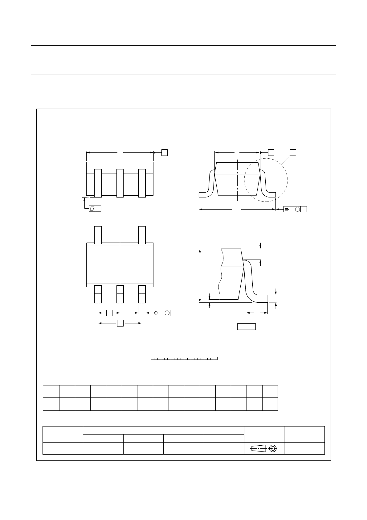
PACKAGE OUTLINE
Plastic surface mounted package; 5 leads SOT353
D
y
E
H
E
AB
45
X
v
M
A
132
e
DIMENSIONS (mm are the original dimensions)
A
1
mm
OUTLINE
VERSION
SOT353
1.1
0.8
A
max
0.1
b
p
0.30
0.20
IEC JEDEC EIAJ
UNIT
b
1
0.25
0.10
p
e
cD
2.2
1.8
A
wB
M
0 1 2 mm
scale
(2)
E
1.35
1.15
REFERENCES
1.3
e
0.65
H
E
1
2.2
0.45
2.0
0.15
e
Q
A
1
L
detail X
L
Qywv
p
0.25
0.15
0.2 0.10.2
EUROPEAN
PROJECTION
c
p
ISSUE DATE
97-02-28SC-88A
2004 Mar 23 7

Philips Semiconductors Product specification
Low capacitance quadruple ESD
PESDxL4UG series
protection diode array in SOT353 package
DATA SHEET STATUS
LEVEL
I Objective data Development This data sheet contains data from the objective specification for product
II Preliminary data Qualification This data sheet contains data from the preliminary specification.
III Product data Production This data sheet contains data from the product specification. Philips
Notes
1. Please consult the most recently issued data sheet before initiating or completing a design.
2. The product status of the device(s) described in this data sheet may have changed since this data sheet was
3. For data sheets describingmultiple typenumbers, thehighest-level product status determines the data sheetstatus.
DATA SHEET
STATUS
published. The latest information is available on the Internet at URL http://www.semiconductors.philips.com.
(1)
PRODUCT
STATUS
(2)(3)
development. Philips Semiconductors reserves the right to change the
specification in any manner without notice.
Supplementary data will be published at a later date. Philips
Semiconductors reserves the right to change the specification without
notice, in order to improve the design and supply the best possible
product.
Semiconductors reserves the right to make changes at any time in order
to improve the design, manufacturing and supply. Relevant changes will
be communicated via a Customer Product/Process Change Notification
(CPCN).
DEFINITION
DEFINITIONS
Short-form specification The data in a short-form
specification is extracted from a full data sheet with the
same type number and title. For detailed information see
the relevant data sheet or data handbook.
Limiting values definition Limiting valuesgiven are in
accordance with the Absolute Maximum Rating System
(IEC 60134). Stress above one or more of the limiting
values may cause permanent damage to the device.
These are stress ratings only and operation of the device
atthese or atany other conditionsabovethose giveninthe
Characteristics sectionsof the specification is not implied.
Exposure to limiting values for extended periods may
affect device reliability.
Application information Applications that are
described herein for any of these products are for
illustrative purposes only. Philips Semiconductors make
norepresentation or warrantythatsuchapplications will be
suitable for the specified use without further testing or
modification.
DISCLAIMERS
Life support applications These products are not
designed for use in life support appliances, devices, or
systems where malfunction of these products can
reasonably be expectedto resultin personalinjury. Philips
Semiconductorscustomers using orsellingtheseproducts
for use in such applications do so at their own risk and
agree to fully indemnify Philips Semiconductors for any
damages resulting from such application.
Right to make changes Philips Semiconductors
reserves the right to make changes in the products including circuits, standard cells, and/or software described or contained herein in order to improve design
and/or performance. When the product is in full production
(status ‘Production’), relevant changes will be
communicated via a Customer Product/Process Change
Notification (CPCN). Philips Semiconductors assumes no
responsibility or liability for the use of any of these
products, conveys no licence or title under any patent,
copyright, or mask work right to these products, and
makes no representations or warranties that these
products are free from patent, copyright, or mask work
right infringement, unless otherwise specified.
2004 Mar 23 8

Philips Semiconductors – a w orldwide compan y
Contact information
For additional information please visit http://www.semiconductors.philips.com. Fax: +31 40 27 24825
For sales offices addresses send e-mail to: sales.addresses@www.semiconductors.philips.com.
© Koninklijke Philips Electronics N.V. 2004
All rights are reserved. Reproduction in whole or in part is prohibited without the prior written consent of the copyright owner.
The information presented in this document does not form part of any quotation or contract, is believed to be accurate and reliable and may be changed
without notice. No liability will be accepted by the publisher for any consequence of its use. Publication thereof does not convey nor imply any license
under patent- or other industrial or intellectual property rights.
Printed in The Netherlands R76/01/pp9 Date of release: 2004 Mar 23 Document order number: 9397 750 12226
SCA76
 Loading...