


查询PESD3V3L2UM供应商
DISCRETE SEMICONDUCTORS
DATA SH EET
M3D883
BOTTOM VIEW
PESDxL2UM series
Low capacitance double ESD
protection diode
Product specification 2003 Aug 05
Philips Semiconductors Product specification
Low capacitance double ESD protection diode PESDxL2UM series
FEATURES
• Uni-directional ESD protection of two lines or
bi-directional ESD protection of one line
• Reverse standoff voltage 3.3 and 5 V
• Low diode capacitance
• Ultra low leakage current
• Leadless ultra small SOT883 surface mount package
(1 × 0.6 × 0.5 mm)
• Board space 1.17 mm2 (approx. 10% of SOT23)
• ESD protection >15 kV
• IEC 61000-4-2; level 4 (ESD); 15 kV (air) or
8 kV (contact).
APPLICATIONS
• Cellular handsets and accessories
• Portable electronics
• Computers and peripherals
• Communication systems
• Audio and video equipment.
MARKING
TYPE NUMBER MARKING CODE
PESD3V3L2UM F2
PESD5V0L2UM F1
DESCRIPTION
Low capacitance ESD protection diode in a three pad
SOT883 leadless ultra small plastic package designed to
protect up to two transmission or data lines from
ElectroStatic Discharge (ESD) damage.
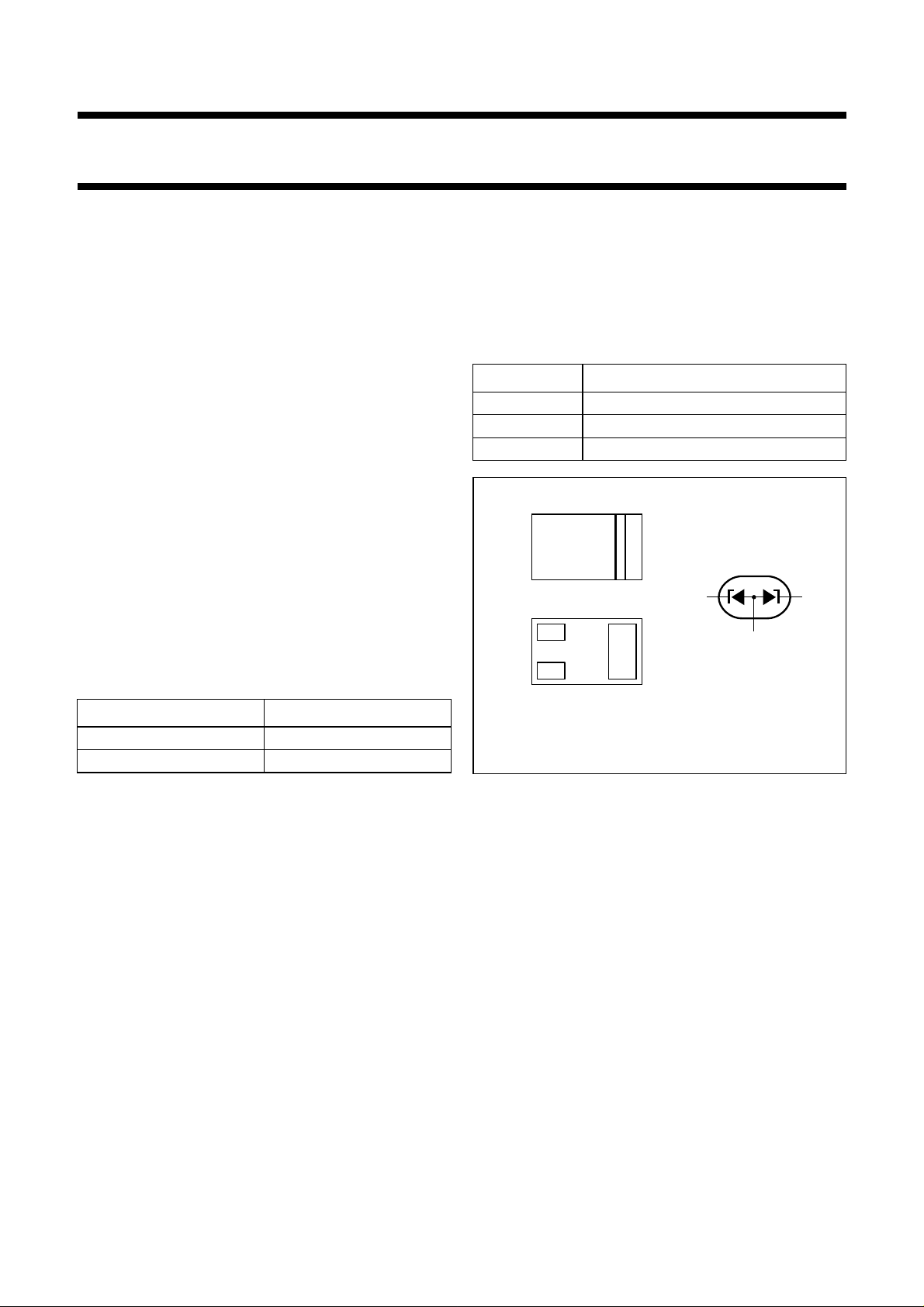
PINNING
PIN DESCRIPTION
1 cathode 1
2 cathode 2
3 common anode
handbook, halfpage
Top view
2
1
Bottom view
2
3
3
MLE220
1
Fig.1 Simplified outline (SOT883) and symbol.
2003 Aug 05 2
Philips Semiconductors Product specification
Low capacitance double ESD protection diode PESDxL2UM series
LIMITING VALUES
In accordance with the Absolute Maximum Rating System (IEC 60134).
SYMBOL PARAMETER CONDITIONS MIN. MAX. UNIT
Per diode
I
pp
P
pp
I
FSM
I
ZSM
P
tot
P
ZSM
T
stg
T
j
ESD electrostatic discharge IEC 61000-4-2 (contact discharge) 15 − kV
peak pulse current 8/20 µs pulse; notes 1, 2 and 3
PESD3V3L2UM − 3A
PESD5V0L2UM − 2.5 A
peak pulse power 8/20 µs pulse; notes 1, 2 and 3 − 30 W
non-repetitive peak forward current tp= 1 ms; square pulse − 3.5 A
non-repetitive peak reverse current tp= 1 ms; square pulse
PESD3V3L2UM − 0.9 A
PESD5V0L2UM − 0.8 A
total power dissipation T
non-repetitive peak reverse power
=25°C; note 4 − 250 mW
amb
tp= 1 ms; square pulse; see Fig.4 − 6W
dissipation
storage temperature −65 +150 °C
junction temperature − 150 °C
HBM MIL-Std 883 10 − kV
Notes
1. Non-repetitive current pulse 8/20 µs exponential decay waveform; see Fig.5.
2. Pins 1 and 3 or 2 and 3.
3. Pins 1 and 2.
4. Device mounted on standard printed-circuit board.
ESD standards compliance
IEC 61000-4-2, level 4 (ESD) >15 kV (air); >8 kV (contact)
HBM MIL-Std 883, class 3 >4 kV
THERMAL CHARACTERISTICS
SYMBOL PARAMETER CONDITIONS VALUE UNIT
R
th j-a
thermal resistance from junction to ambient all diodes loaded; note 1 500 K/W
one diode loaded; note 2 290 K/W
Notes
1. Refer to SOT883 standard mounting conditions (footprint), FR4 with 60 µm copper strip line.
2. FR4 single-sided copper 1 cm
2
.
2003 Aug 05 3

Philips Semiconductors Product specification
Low capacitance double ESD protection diode PESDxL2UM series
ELECTRICAL CHARACTERISTICS
Tj=25°C unless otherwise specified.
SYMBOL PARAMETER CONDITIONS MIN. TYP. MAX. UNIT
Per diode
V
F
V
RWM
I
RM
V
(CL)R
V
BR
S
Z
r
diff
C
d
forward voltage IF= 200 mA − 1 1.2 V
reverse stand-off voltage
PESD3V3L2UM −−3.3 V
PESD5V0L2UM −−5V
reverse leakage current
PESD3V3L2UM V
PESD5V0L2UM V
= 3.3 V − 75 300 nA
R
=5V − 525nA
R
clamping voltage 8/20 µs pulse
PESD3V3L2UM I
PESD5V0L2UM I
= 1 A; notes 1 and 2 −−8V
pp
I
= 3 A; notes 1 and 2 −−12 V
pp
I
= 1 A; notes 1 and 3 −−9V
pp
I
= 3 A; notes 1 and 3 −−13 V
pp
= 1 A; notes 1 and 2 −−10 V
pp
I
= 2.5 A; notes 1 and 2 −−13 V
pp
I
= 1 A; notes 1 and 3 −−11 V
pp
I
= 2.5 A; notes 1 and 3 −−15 V
pp
breakdown voltage IZ=1mA
PESD3V3L2UM 5.32 5.6 5.88 V
PESD5V0L2UM 6.46 6.8 7.14 V
temperature coefficient IZ=1mA
PESD3V3L2UM − 1.3 − mV/K
PESD5V0L2UM − 2.9 − mV/K
differential resistance IR=1mA
PESD3V3L2UM −−200 Ω
PESD5V0L2UM −−100 Ω
diode capacitance
PESD3V3L2UM f = 1 MHz; V
f = 1 MHz; V
PESD5V0L2UM f = 1 MHz; V
f = 1 MHz; V
=0 − 22 28 pF
R
=5 − 12 17 pF
R
=0 − 16 19 pF
R
=5 − 811pF
R
Notes
1. Non-repetitive current pulse 8/20 µs exponential decay waveform; see Fig.5.
2. Pins 1 and 3 or 2 and 3.
3. Pins 1 and 2.
2003 Aug 05 4

Philips Semiconductors Product specification
Low capacitance double ESD protection diode PESDxL2UM series
10
handbook, halfpage
I
ZSM
(A)
1
−1
10
−2
10
−1
10
PESD3V3L2UM
PESD5V0L2UM
1
MLE215
tp (ms)
Fig.2 Non-repetitive peak reverse current as a
function of pulse time (square pulse).
26
handbook, halfpage
C
d
(pF)
22
18
14
10
10
6
05
Tj=25°C; f = 1 MHz.
1234
PESD3V3L2UM
PESD5V0L2UM
MLE216
V
(V)
R
Fig.3 Diode capacitance as a function of reverse
voltage; typical values.
2
10
handbook, halfpage
P
ZSM
(W)
PESD3V3L2UM
10
PESD5V0L2UM
1
−2
10
P
= V
ZSM
ZSMxIZSM
V
is the non-repetitive peak reverse voltage at I
ZSM
−1
10
.
1
tp (ms)
ZSM
Fig.4 Maximum non-repetitive peak reverse
power dissipation as a function of pulse
duration (square pulse).
MLE217
.
120
handbook, halfpage
I
pp
(%)
80
40
10
0
010
100 % Ipp; 8 µs
−t
e
20
50 % Ipp; 20 µs
MLE218
t (µs)
40
30
Fig.5 8/20 µs pulse waveform according to
IEC 61000-4-5.
2003 Aug 05 5

Philips Semiconductors Product specification
Low capacitance double ESD protection diode PESDxL2UM series
handbook, full pagewidth
Note 1: IEC 61000-4-2 network
CZ = 150 pF; RZ = 330 Ω
GND
ESD TESTER 4 GHz DIGITAL
R
Z
C
Z
note 1
vertical scale = 200 V/div
horizontal scale = 50 ns/div
450 Ω
12
3
RG 223/U
50 Ω coax
D.U.T
PESDxL2UM
GND2
GND1
10×
ATTENUATOR
PESD5V0L2UM
PESD3V3L2UM
OSCILLOSCOPE
50 Ω
vertical scale = 5 V/div
horizontal scale = 50 ns/div
unclamped +1 kV ESD voltage waveform
(IEC 61000-4-2 network)
GND
vertical scale = 200 V/div
horizontal scale = 50 ns/div
unclamped −1 kV ESD voltage waveform
(IEC 61000-4-2 network)
clamped +1 kV ESD voltage waveform
(IEC 61000-4-2 network)
GND
clamped −1 kV ESD voltage waveform
(IEC 61000-4-2 network)
Fig.6 ESD clamping test set-up and waveforms.
vertical scale = 5 V/div
horizontal scale = 50 ns/div
MLE219
2003 Aug 05 6

Philips Semiconductors Product specification
Low capacitance double ESD protection diode PESDxL2UM series
PACKAGE OUTLINE
Leadless ultra small plastic package; 3 solder lands; body 1.0 x 0.6 x 0.5 mm SOT883
L
2
b
e
1
e
1
E
L
1
3
b
1
A
A
1
DIMENSIONS (mm are the original dimensions)
A
(1)
UNIT
A
0.50
mm
0.46
Note
1. Including plating thickness
OUTLINE
VERSION
SOT883 SC-101
max.
0.03
1
bb
0.20
0.12
IEC JEDEC JEITA
1
0.55
0.47
DE
0.62
0.55
eLL
1.02
0.35 0.65
0.95
REFERENCES
e
1
0.30
0.22
2003 Aug 05 7
D
1
0.30
0.22
0 0.5 1 mm
scale
EUROPEAN
PROJECTION
ISSUE DATE
03-02-05
03-04-03

Philips Semiconductors Product specification
Low capacitance double ESD protection diode PESDxL2UM series
DATA SHEET STATUS
LEVEL
DATA SHEET
STATUS
(1)
PRODUCT
STATUS
(2)(3)
DEFINITION
I Objective data Development This data sheet contains data from the objective specification for product
development. Philips Semiconductors reserves the right to change the
specification in any manner without notice.
II Preliminary data Qualification This data sheet contains data from the preliminary specification.
Supplementary data will be published at a later date. Philips
Semiconductors reserves the right to change the specification without
notice, in order to improve the design and supply the best possible
product.
III Product data Production This data sheet contains data from the product specification. Philips
Semiconductors reserves the right to make changes at any time in order
to improve the design, manufacturing and supply. Relevant changes will
be communicated via a Customer Product/Process Change Notification
(CPCN).
Notes
1. Please consult the most recently issued data sheet before initiating or completing a design.
2. The product status of the device(s) described in this data sheet may have changed since this data sheet was
published. The latest information is available on the Internet at URL http://www.semiconductors.philips.com.
3. For data sheets describing multiple type numbers, the highest-levelproduct statusdetermines thedata sheetstatus.
DEFINITIONS
DISCLAIMERS
Short-form specification The data in a short-form
specification is extracted from a full data sheet with the
same type number and title. For detailed information see
the relevant data sheet or data handbook.
Limiting values definition Limiting values given are in
accordance with the Absolute Maximum Rating System
(IEC 60134). Stress above one or more of the limiting
values may cause permanent damage to the device.
These are stress ratings only and operation of the device
atthese or at anyotherconditions above those giveninthe
Characteristics sections of the specification is not implied.
Exposure to limiting values for extended periods may
affect device reliability.
Application information Applications that are
described herein for any of these products are for
illustrative purposes only. Philips Semiconductors make
norepresentationor warranty that such applications willbe
suitable for the specified use without further testing or
modification.
Life support applications These products are not
designed for use in life support appliances, devices, or
systems where malfunction of these products can
reasonably be expectedto result inpersonal injury. Philips
Semiconductorscustomersusingor selling these products
for use in such applications do so at their own risk and
agree to fully indemnify Philips Semiconductors for any
damages resulting from such application.
Right to make changes Philips Semiconductors
reserves the right to make changes in the products including circuits, standard cells, and/or software described or contained herein in order to improve design
and/or performance. Whenthe product is in full production
(status ‘Production’), relevant changes will be
communicated via a Customer Product/Process Change
Notification (CPCN). Philips Semiconductors assumes no
responsibility or liability for the use of any of these
products, conveys no licence or title under any patent,
copyright, or mask work right to these products, and
makes no representations or warranties that these
products are free from patent, copyright, or mask work
right infringement, unless otherwise specified.
2003 Aug 05 8

Philips Semiconductors – a w orldwide compan y
Contact information
For additional information please visit http://www.semiconductors.philips.com. Fax: +31 40 27 24825
For sales offices addresses send e-mail to: sales.addresses@www.semiconductors.philips.com.
© Koninklijke Philips Electronics N.V. 2003
All rights are reserved. Reproduction in whole or in part is prohibited without the prior written consent of the copyright owner.
The information presented in this document does not form part of any quotation or contract, is believed to be accurate and reliable and may be changed
without notice. No liability will be accepted by the publisher for any consequence of its use. Publication thereof does not convey nor imply any license
under patent- or other industrial or intellectual property rights.
Printed in The Netherlands 613514/01/pp9 Date of release: 2003 Aug 05 Document order number: 9397 750 11644
SCA75
 Loading...