


查询PESD5V2S18U供应商
DISCRETE SEMICONDUCTORS
DATA SH EET
M3D574
PESD5V2S18U
ESD protection array
Product specification 2003 Apr 28
Philips Semiconductors Product specification
ESD protection array PESD5V2S18U
FEATURES
• Uni-directional ESD protection of
up to 18 lines
• Maximum peak reverse power:
PPP= 100 W at tp= 8/20 µs
• Low clamping voltage:
VCL= 12 V max. at I
ZSM
=10A
• Low leakage current:
IR= 100 nA typ. at V
RWM
= 5.2 V
• IEC 61000-4-2, level 4 (ESD);
15 kV (air) and 8 kV (contact).
APPLICATIONS
• Printer parallel ports
• Computers and peripherals
• Communication systems.
DESCRIPTION
Monolithic ESD protection device
designed to protect up to
18 transmissionordatalinesfromthe
damage caused by electrostatic
discharge (ESD) and surge pulses.
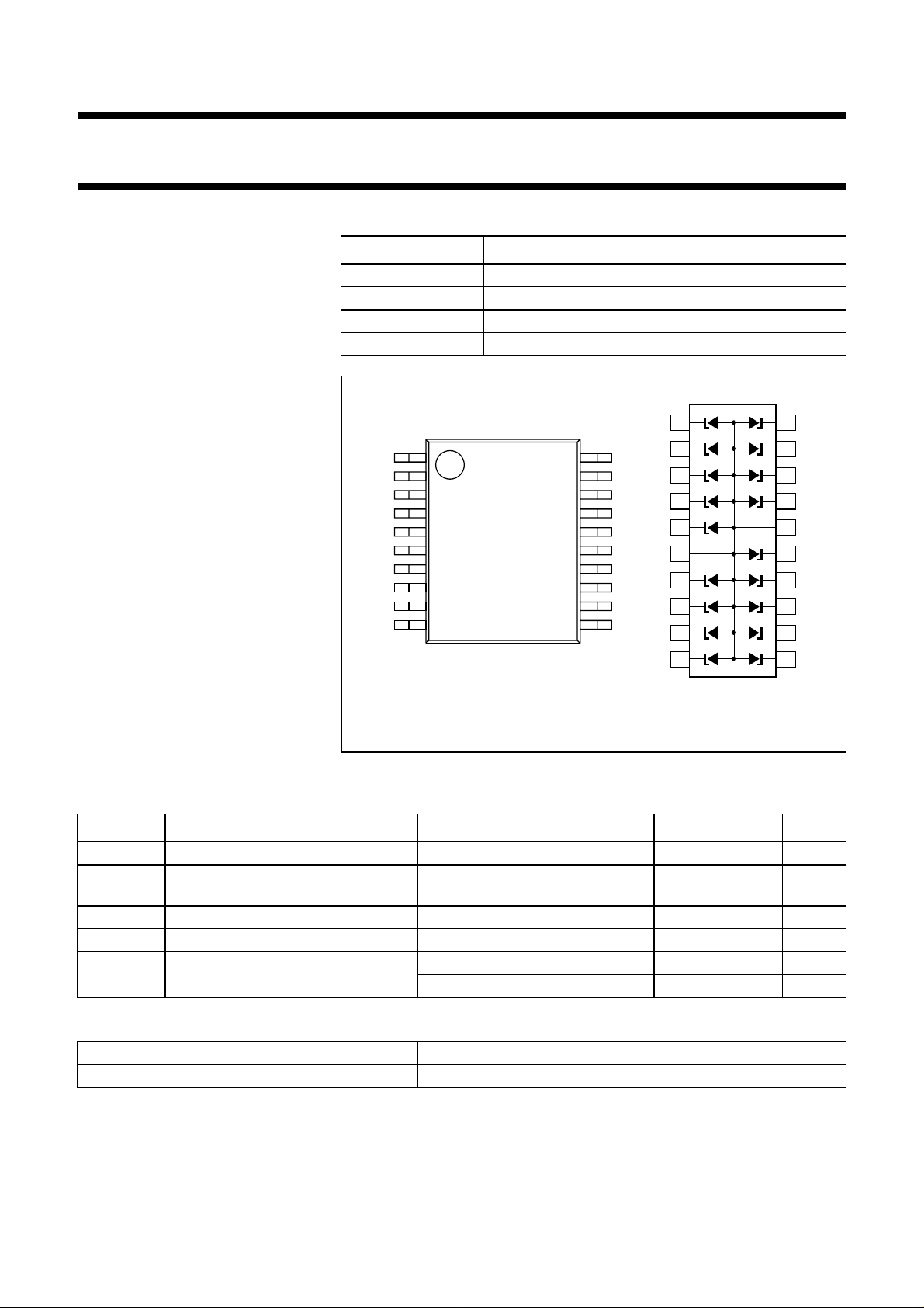
PINNING
PIN DESCRIPTION
1 to 5 cathode (k1 to k5)
6 and 16 common anode (a1; a2)
7 to 15 cathode (k6 to k14)
17 to 20 cathode (k15 to k18)
handbook, 4 columns
1
10
Fig.1 Simplified outline (SSOP20; SOT339-1) and symbol.
1
20
11
2
3
4
5
6
7
8
9
10
20
19
18
17
16
15
14
13
12
11
MHC510
LIMITING VALUES
In accordance with the Absolute Maximum Rating System (IEC 60134).
SYMBOL PARAMETER CONDITIONS MIN. MAX. UNIT
I
PP
P
PP
non-repetitive peak reverse current tp= 8/20 µs − 10 A
non-repetitive peak reverse power
tp= 8/20 µs − 100 W
dissipation
T
stg
T
j
storage temperature −65 +150 °C
junction temperature −65 +150 °C
electrostatic discharge voltage IEC 61000-4-2 (contact discharge) 30 − kV
HBM MIL-Std 883 10 − kV
ESD standards compliance
IEC 61000-4-2, level 4 (ESD) >15 kV (air); >8 kV (contact)
HBM MIL-Std 883, class 3 >4 kV
2003 Apr 28 2
Philips Semiconductors Product specification
ESD protection array PESD5V2S18U
THERMAL CHARACTERISTICS
SYMBOL PARAMETER CONDITIONS VALUE UNIT
R
th j-a
Note
1. Refer to SOT339-1 standard mounting conditions.
ELECTRICAL CHARACTERISTICS
T
=25°C unless otherwise specified.
amb
SYMBOL PARAMETER CONDITIONS MIN. TYP. MAX. UNIT
V
RWM
I
R
V
CL
V
BR
r
diff
C
d
thermal resistance from junction to
one or more diodes loaded 135 K/W
ambient
crest working reverse
−−5.2 V
voltage
reverse current V
clamping voltage I
= 5.2 V − 0.1 1 µA
RWM
= 3 A; tp= 8/20 µs; see Fig.5 −−8V
ZSM
I
= 10 A; tp= 8/20 µs; see Fig.5 −−12 V
ZSM
breakdown voltage IZ= 5 mA 6.4 6.8 7.2 V
differential resistance IZ=1mA −−40 Ω
I
=5mA −−8Ω
Z
diode capacitance VR= 0; f = 1 MHz; see Fig.4 − 100 − pF
2003 Apr 28 3

Philips Semiconductors Product specification
ESD protection array PESD5V2S18U
3
10
handbook, halfpage
P
ZSM
(W)
2
10
10
−2
10
−1
10
110
t
(ms)
p
Fig.2 Maximum non-repetitive peak reverse
power as a function of pulse duration.
MHC485
2
10
handbook, halfpage
I
ZSM
(A)
10
1
−2
10
−1
10
110
t
(ms)
p
Fig.3 Maximum non-repetitive peak reverse
current as a function of pulse duration.
MHC486
110
handbook, halfpage
C
d
(pF)
100
90
80
70
60
50
40
01
f = 1 MHz; T
amb
35
26
=25°C
4
MHC487
V
(V)
R
Fig.4 Diode capacitance as a function of reverse
voltage; typical values.
2003 Apr 28 4
11
handbook, halfpage
V
CL
(V)
10
9
8
7
3 56789104
tp= 8/20 µs
Fig.5 Clamping voltage as a function of peak
reverse pulse current; typical values.
MHC488
IPP(A)

Philips Semiconductors Product specification
ESD protection array PESD5V2S18U
IEC 1000-4-2 network
CZ = 150 pF; RZ = 330 Ω
GND
ESD TESTER DIGITIZING
R
Z
C
Z
1/18 PESD5V2S18U
vertical scale = 200 V/Div
horizontal scale = 50 ns/Div
450 Ω
RG 223/U
50 Ω coax
GND
10×
ATTENUATOR
note 1
Note 1: attenuator is only used for open
socket high voltage measurements
vertical scale = 5 V/Div
horizontal scale = 50 ns/Div
OSCILLOSCOPE
50 Ω
unclamped +1 kV ESD voltage waveform
(IEC 1000−4−2 network)
GND
vertical scale = 200 V/Div
horizontal scale = 50 ns/Div
unclamped −1 kV ESD voltage waveform
(IEC 1000−4−2 network)
Fig.6 ESD clamping test set-up and waveforms.
2003 Apr 28 5
clamped +1 kV ESD voltage waveform
(IEC 1000−4−2 network)
GND
vertical scale = 5 V/Div
horizontal scale = 50 ns/Div
clamped −1 kV ESD voltage waveform
(IEC 1000−4−2 network)
MHC489

Philips Semiconductors Product specification
ESD protection array PESD5V2S18U
PACKAGE OUTLINE
SSOP20: plastic shrink small outline package; 20 leads; body width 5.3 mm
SOT339-1
D
c
y
Z
20 11
A
2
A
pin 1 index
110
w M
b
e
p
1
E
H
E
detail X
A
X
v M
A
Q
(A )
L
p
L
A
3
θ
0 2.5 5 mm
scale
DIMENSIONS (mm are the original dimensions)
UNIT A1A2A
Note
1. Plastic or metal protrusions of 0.2 mm maximum per side are not included.
A
max.
0.21
mm
2
OUTLINE
VERSION
SOT339-1 MO-150
0.05
1.80
1.65
IEC JEDEC JEITA
0.25
b
3
p
0.38
0.20
0.25
0.09
(1)E(1)
cD
7.4
7.0
REFERENCES
5.4
5.2
2003 Apr 28 6
eHELLpQ
0.65
7.9
7.6
1.03
0.63
0.9
0.7
0.131.25 0.2 0.1
EUROPEAN
PROJECTION
(1)
Zywv θ
0.9
0.5
ISSUE DATE
99-12-27
03-02-19
o
8
o
0

Philips Semiconductors Product specification
ESD protection array PESD5V2S18U
DATA SHEET STATUS
LEVEL
DATA SHEET
STATUS
(1)
PRODUCT
STATUS
(2)(3)
DEFINITION
I Objective data Development This data sheet contains data from the objective specification for product
development. Philips Semiconductors reserves the right to change the
specification in any manner without notice.
II Preliminary data Qualification This data sheet contains data from the preliminary specification.
Supplementary data will be published at a later date. Philips
Semiconductors reserves the right to change the specification without
notice, in order to improve the design and supply the best possible
product.
III Product data Production This data sheet contains data from the product specification. Philips
Semiconductors reserves the right to make changes at any time in order
to improve the design, manufacturing and supply. Relevant changes will
be communicated via a Customer Product/Process Change Notification
(CPCN).
Notes
1. Please consult the most recently issued data sheet before initiating or completing a design.
2. The product status of the device(s) described in this data sheet may have changed since this data sheet was
published. The latest information is available on the Internet at URL http://www.semiconductors.philips.com.
3. For data sheets describing multiple type numbers, the highest-level product status determines the data sheet status.
DEFINITIONS
DISCLAIMERS
Short-form specification The data in a short-form
specification is extracted from a full data sheet with the
same type number and title. For detailed information see
the relevant data sheet or data handbook.
Limiting values definition Limiting values given are in
accordance with the Absolute Maximum Rating System
(IEC 60134). Stress above one or more of the limiting
values may cause permanent damage to the device.
These are stress ratings only and operation of the device
attheseoratanyotherconditionsabovethosegiveninthe
Characteristics sections of the specification is not implied.
Exposure to limiting values for extended periods may
affect device reliability.
Application information Applications that are
described herein for any of these products are for
illustrative purposes only. Philips Semiconductors make
norepresentationorwarrantythatsuchapplicationswill be
suitable for the specified use without further testing or
modification.
Life support applications These products are not
designed for use in life support appliances, devices, or
systems where malfunction of these products can
reasonably be expected to result in personal injury. Philips
Semiconductorscustomers using or selling theseproducts
for use in such applications do so at their own risk and
agree to fully indemnify Philips Semiconductors for any
damages resulting from such application.
Right to make changes Philips Semiconductors
reserves the right to make changes in the products including circuits, standard cells, and/or software described or contained herein in order to improve design
and/or performance. When the product is in full production
(status ‘Production’), relevant changes will be
communicated via a Customer Product/Process Change
Notification (CPCN). Philips Semiconductors assumes no
responsibility or liability for the use of any of these
products, conveys no licence or title under any patent,
copyright, or mask work right to these products, and
makes no representations or warranties that these
products are free from patent, copyright, or mask work
right infringement, unless otherwise specified.
2003 Apr 28 7

Philips Semiconductors – a w orldwide compan y
Contact information
For additional information please visit http://www.semiconductors.philips.com. Fax: +31 40 27 24825
For sales offices addresses send e-mail to: sales.addresses@www.semiconductors.philips.com.
© Koninklijke Philips Electronics N.V. 2003
All rights are reserved. Reproduction in whole or in part is prohibited without the prior written consent of the copyright owner.
The information presented in this document does not form part of any quotation or contract, is believed to be accurate and reliable and may be changed
without notice. No liability will be accepted by the publisher for any consequence of its use. Publication thereof does not convey nor imply any license
under patent- or other industrial or intellectual property rights.
Printed in The Netherlands 613514/01/pp8 Date of release: 2003 Apr 28 Document order number: 9397 750 10889
SCA75
 Loading...