

Philips PESD3V3L5UV, PESD5V0L5UV User Manual

查询PESD3V3L5UV供应商
DISCRETE SEMICONDUCTORS
DATA SH EET
M3D744
PESD3V3L5UV; PESD5V0L5UV
Low capacitance 5-fold ESD
protection diode arrays in SOT666
package
Product specification 2004 Mar 23
Philips Semiconductors Product specification
Low capacitance 5-fold ESD protection
diode arrays in SOT666 package
FEATURES
• Uni-directional ESD protection of up to five lines
• Bi-directional ESD protection of up to four lines
• Low diode capacitance
• Maximum peak pulse power: Ppp= 25 W at tp= 8/20µs
• Low clamping voltage: V
• Ultra low leakage current: IRM= 8 nA at V
• ESD protection > 20 kV
• IEC 61000-4-2; level 4 (ESD)
• IEC 61000-4-5 (surge); Ipp= 2.5 A at Tp= 8/20 µs.
APPLICATIONS
• Cellular handsets and accessories
• Portable electronics
• Computers and peripherals
• Communications systems
• Audio and video equipment.
DESCRIPTION
= 12 V at Ipp= 2.5 A
CL(R)
RWM
=5V
PESD3V3L5UV;
PESD5V0L5UV
QUICK REFERENCE DATA
SYMBOL PARAMETER VALUE UNIT
V
RWM
C
d
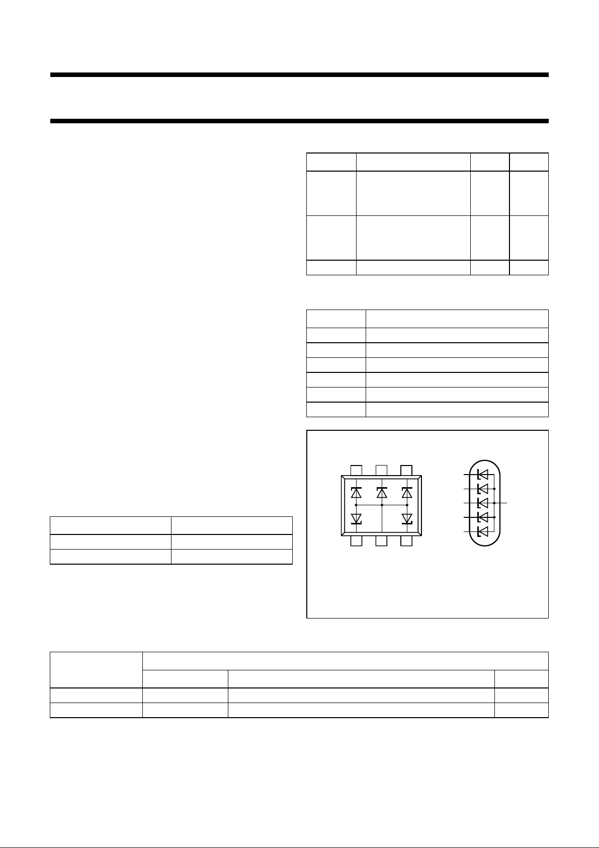
PINNING
PIN DESCRIPTION
reverse standoff voltage
PESD3V3L5UV 3.3 V
PESD5V0L5UV 5 V
diode capacitance
PESD3V3L5UV 22 pF
PESD5V0L5UV 16 pF
number of protected lines 5
1 cathode 1
2 common anode
3 cathode 2
4 cathode 3
5 cathode 4
6 cathode 5
Low capacitance 5-fold ESD protection array in the ultra
small SOT666 plastic package designed to protect up to
five transmissionor data lines from the damage caused by
Electrostatic Discharge (ESD).
MARKING
TYPE NUMBER MARKING CODE
(1)
456
1
3
42
5
6
PESD3V3L5UV *E1
PESD5V0L5UV *E2
132
001aaa213
sym011
Note
1. * = p: Made in Hong Kong.
* = t: Made in Malaysia.
Fig.1 Simplified outline (SOT666) and symbol.
* = W: Made in China.
ORDERING INFORMATION
PACKAGE
TYPE NUMBER
NAME DESCRIPTION VERSION
PESD3V3L5UV − plastic surface mounted package; 6 leads SOT666
PESD5V0L5UV − plastic surface mounted package; 6 leads SOT666
2004 Mar 23 2

Philips Semiconductors Product specification
Low capacitance 5-fold ESD protection
diode arrays in SOT666 package
LIMITING VALUES
In accordance with the Absolute Maximum Rating System (IEC 60134).
SYMBOL PARAMETER CONDITIONS MIN. MAX. UNIT
Per diode
P
pp
I
pp
T
j
T
amb
T
stg
Notes
1. Non-repetitive current pulse 8/20 µs exponentially decaying waveform; see Fig.2.
2. Measured from any of pins 1, 3, 4, 5 or 6 to pin 2.
ESD maximum ratings
SYMBOL PARAMETER CONDITIONS VALUE UNIT
Per diode
ESD electrostatic discharge capability IEC 61000-4-2 (contact
peak pulse power 8/20 µs pulse; notes 1 and 2 − 25 W
peak pulse current 8/20 µs pulse; notes 1 and 2 − 2.5 A
junction temperature − 150 °C
operation ambient temperature −65 +150 °C
storage temperature −65 +150 °C
discharge); notes 1 and 2
HBM MIL-Std 883 10 kV
PESD3V3L5UV;
PESD5V0L5UV
20 kV
Notes
1. Device stressed with ten non-repetitive Electrostatic Discharge (ESD) pulses; see Fig.3.
2. Measured from any of pins 1, 3, 4, 5 or 6 to pin 2.
ESD standards compliance
ESD STANDARD CONDITIONS
IEC 61000-4-2, level 4 (ESD) > 15 kV (air); > 8 kV (contact)
HBM MIL-Std 883, class 3 > 4 kV
2004 Mar 23 3
Philips Semiconductors Product specification
Low capacitance 5-fold ESD protection
diode arrays in SOT666 package
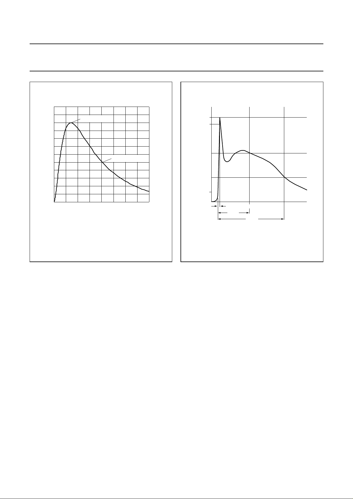
120
handbook, halfpage
I
pp
(%)
80
40
0
010
100 % Ipp; 8 µs
−t
e
20
50 % Ipp; 20 µs
MLE218
t (µs)
40
30
100 %
90 %
10 %
PESD3V3L5UV;
PESD5V0L5UV
001aaa191
I
pp
tr = 0.7 to 1 ns
30 ns
60 ns
t
Fig.2 8/20 µs pulse waveform according to
IEC 61000-4-5.
Fig.3 Electrostatic Discharge (ESD) pulse
waveform according to IEC 61000-4-2.
2004 Mar 23 4
 Loading...