

Philips PEMT1 Datasheet
DISCRETE SEMICONDUCTORS
DATA SH EET
M3D744
PEMT1
PNP general purpose double
transistor
Product specification
Supersedes data of 2001 Sep 25
2001 Nov 07
Philips Semiconductors Product specification
PNP general purpose double transistor PEMT1
FEATURES
• 300 mW total power dissipation
• Very small 1.6 × 1.2 mm ultra thin package
• Self alignment during soldering due to straight leads
• Replaces two SC-75/SC-89 packaged transistors on
same PCB area
• Reduced required PCB area
• Reduced pick and place costs.
APPLICATIONS
• General purpose switching and amplification.
DESCRIPTION
PNP transistor pair in a SOT666 plastic package.
NPN complement: PEMX1.
MARKING
TYPE NUMBER MARKING CODE
PEMT1 FF
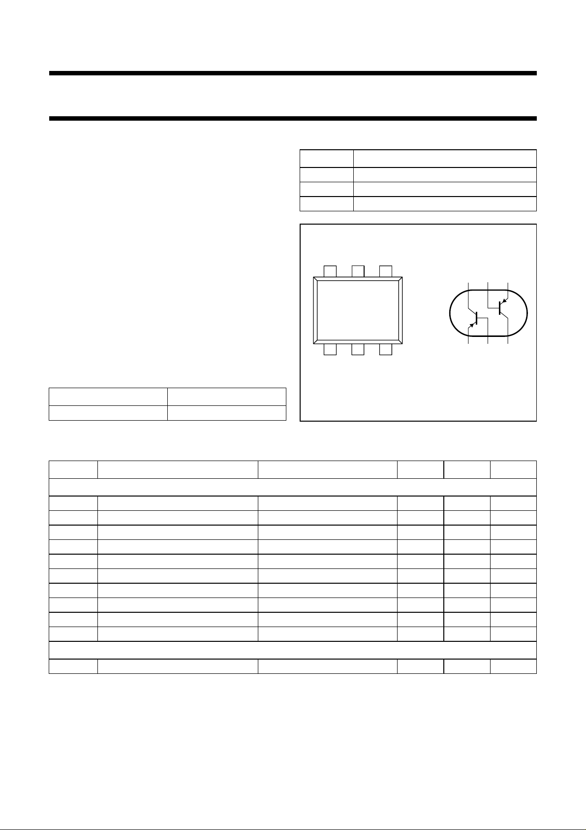
PINNING
PIN DESCRIPTION
1, 4 emitter TR1; TR2
2, 5 base TR1; TR2
6, 3 collector TR1; TR2
465
TR1
123
Top view
MAM450
Fig.1 Simplified outline (SOT666) and symbol.
645
TR2
132
LIMITING VALUES
In accordance with the Absolute Maximum Rating System (IEC 60134).
SYMBOL PARAMETER CONDITIONS MIN. MAX. UNIT
Per transistor
V
CBO
V
CEO
V
EBO
I
C
I
CM
I
BM
P
tot
T
stg
T
j
T
amb
collector-base voltage open emitter −−50 V
collector-emitter voltage open base −−40 V
emitter-base voltage open collector −−5V
collector current (DC) −−100 mA
peak collector current −−200 mA
peak base current −−200 mA
total power dissipation T
≤ 25 °C; note 1 − 200 mW
amb
storage temperature −65 +150 °C
junction temperature − 150 °C
operating ambient temperature −65 +150 °C
Per device
P
tot
total power dissipation T
≤ 25 °C; note 1 − 300 mW
amb
Note
1. Transistor mounted on an FR4 printed-circuit board.
2001 Nov 07 2
Philips Semiconductors Product specification
PNP general purpose double transistor PEMT1
THERMAL CHARACTERISTICS
SYMBOL PARAMETER CONDITIONS VALUE UNIT
R
th j-a
Notes
1. Transistor mounted on an FR4 printed-circuit board.
2. The only recommended soldering is reflow soldering.
CHARACTERISTICS
T
=25°C; unless otherwise specified.
amb
SYMBOL PARAMETER CONDITIONS MIN. MAX. UNIT
Per transistor
I
CBO
I
EBO
h
FE
V
CEsat
C
c
f
T
thermal resistance from junction to ambient notes 1 and 2 416 K/W
collector-base cut-off current VCB= −30 V; IE=0 −−100 nA
= −30 V; IE= 0; Tj= 150 °C −−10 µA
V
CB
emitter-base cut-off current VEB= −4 V; IC=0 −−100 nA
DC current gain VCE= −6 V; IC= −1 mA 120 −
collector-emitter saturation
IC= −50 mA; IB= −5 mA; note 1 −−200 mV
voltage
collector capacitance VCB= −12 V; IE=Ie= 0; f = 1 MHz − 2.2 pF
transition frequency VCE= −12 V; IC= −2 mA;
100 − MHz
f = 100 MHz
Note
1. Pulse test: t
400
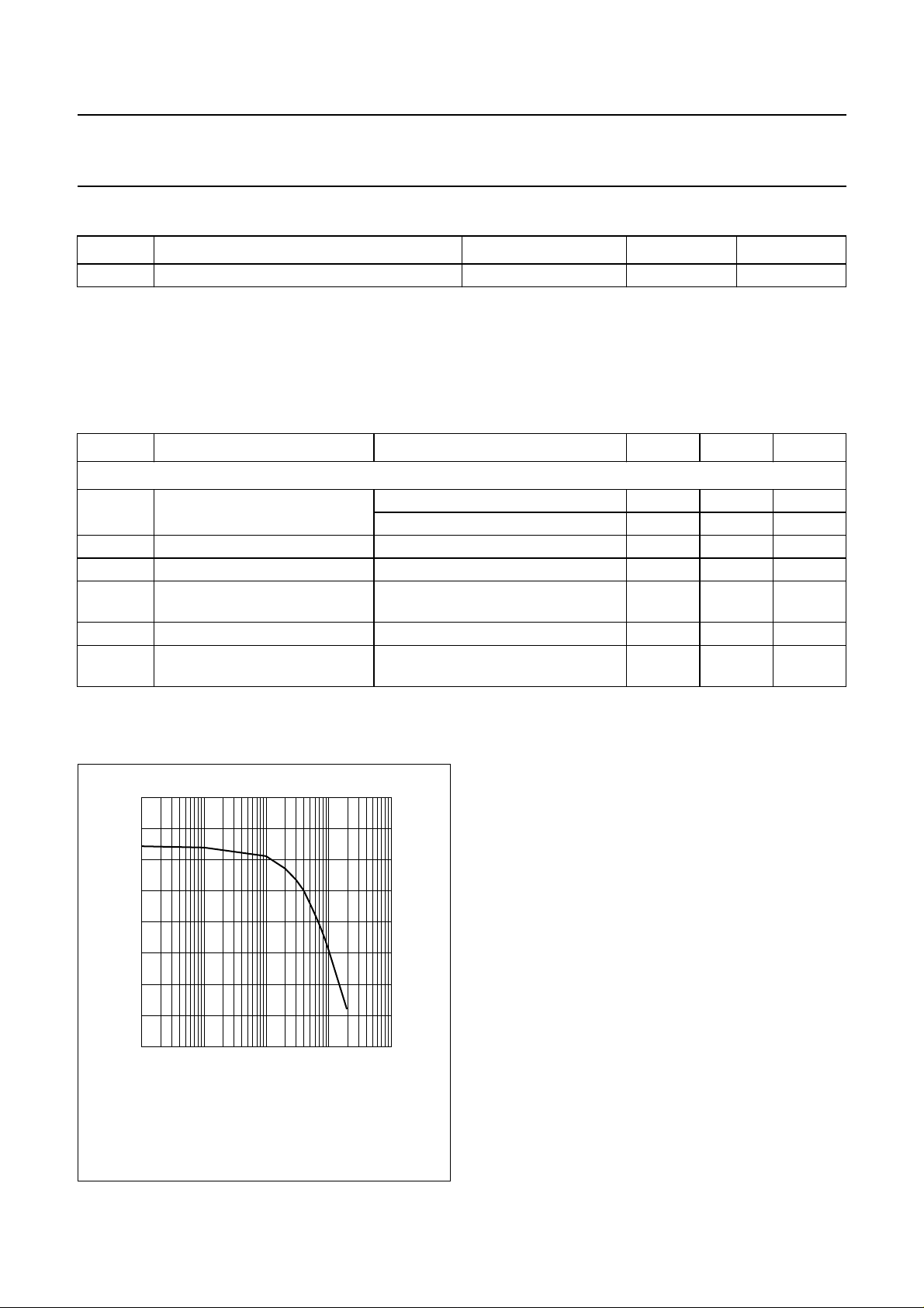
handbook, halfpage
h
FE
300
200
100
0
−10
VCE= −5V.
≤ 300 µs; δ≤0.02.
p
−1
−1 −10
−10
2
IC (mA)
Fig.2 DC current gain as a function of collector
current; typical values.
MHB987
−10
3
2001 Nov 07 3
 Loading...