

Philips PEMD2 Datasheet
DISCRETE SEMICONDUCTORS
DATA SH EET
M3D744
PEMD2
NPN/PNP resistor-equipped
transistors; R1 = 22 kΩ, R2 = 22 kΩ
Preliminary specification 2001 Sep 27
Philips Semiconductors Preliminary specification
NPN/PNP resistor-equipped transistors;
R1 = 22 kΩ, R2 = 22 kΩ
FEATURES
• 300 mW total power dissipation
• Very small 1.6 mm x 1.2 mm ultra thin package
• Self alignment during soldering due to straight leads
• Replaces two SC-75/SC-89 packaged transistors on
same PCB area
• Reduces required PCB area
• Reduced pick and place costs.
APPLICATIONS
• General purpose switching and amplification
• Inverter and interface circuits
• Circuit driver.
DESCRIPTION
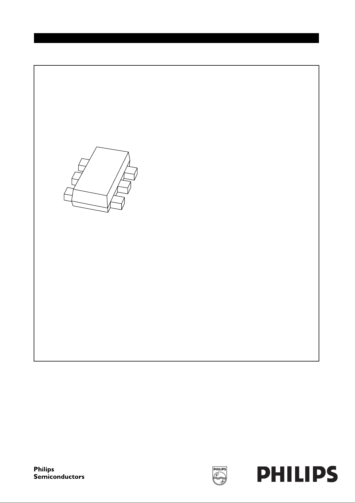
NPN/PNP resistor-equipped transistors in a SOT666
plastic package.
PEMD2
QUICK REFERENCE DATA
SYMBOL PARAMETER MAX. UNIT
V
CEO
I
CM
TR1 NPN −−
TR2 PNP −−
R1 bias resistor 22 kΩ
R2 bias resistor 22 kΩ
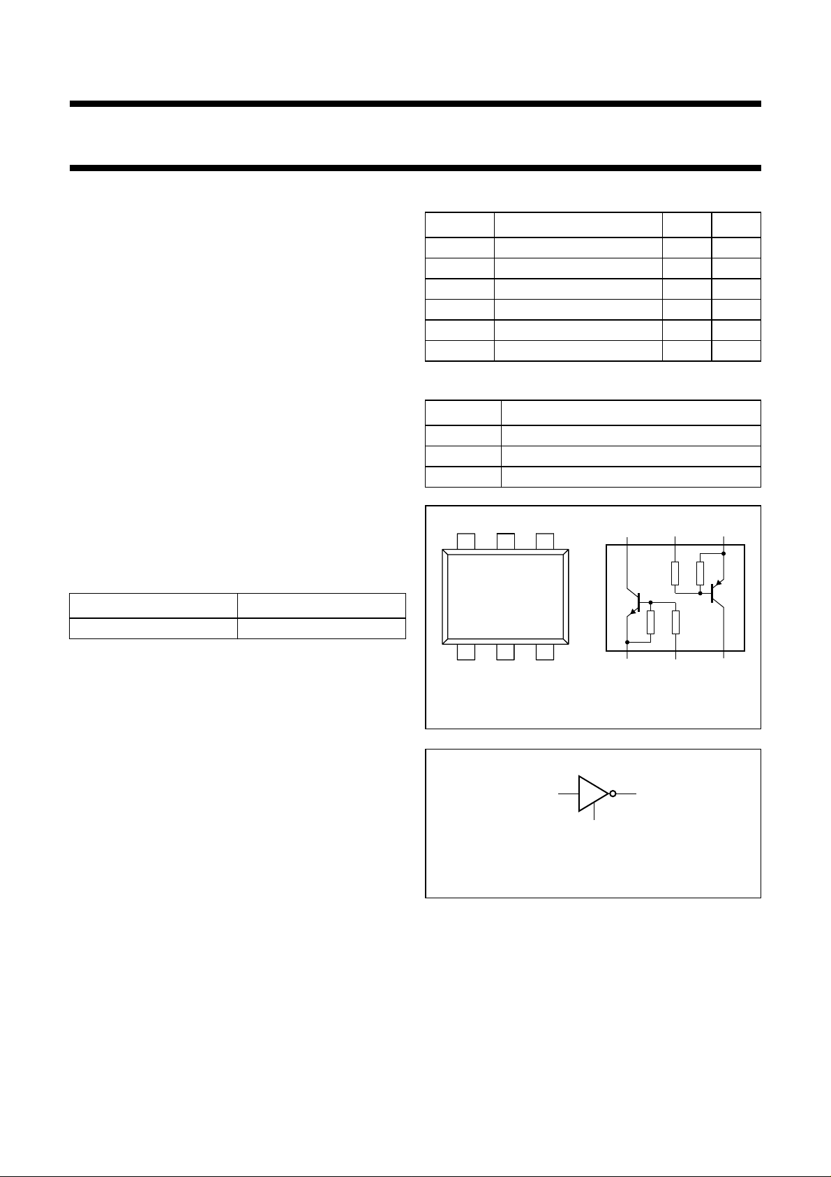
PINNING
PIN DESCRIPTION
1, 4 emitter TR1; TR2
2, 5 base TR1; TR2
6, 3 collector TR1; TR2
handbook, halfpage
collector-emitter voltage 50 V
peak collector current 100 mA
5
46
654
MARKING
TYPE NUMBER MARKING CODE
PEMD2 D4
R1 R2
TR1
R2
R1
123
Top view
MAM448
123
Fig.1 Simplified outline (SOT666) and symbol.
2, 5
1, 4
MBK120
6, 3
Fig.2 Equivalent inverter symbol.
TR2
2001 Sep 27 2

Philips Semiconductors Preliminary specification
NPN/PNP resistor-equipped transistors;
PEMD2
R1 = 22 kΩ, R2 = 22 kΩ
LIMITING VALUES
In accordance with the Absolute Maximum Rating System (IEC 60134).
SYMBOL PARAMETER CONDITIONS MIN. MAX. UNIT
Per transistor; for the PNP transistor with negative polarity
V
CBO
V
CEO
V
EBO
V
I
I
O
I
CM
P
tot
T
stg
T
j
T
amb
Per device
P
tot
collector-base voltage open emitter − 50 V
collector-emitter voltage open base − 50 V
emitter-base voltage open collector − 10 V
input voltage TR1
positive − +40 V
negative −−10 V
input voltage TR2
positive − +10 V
negative −−40 V
output current (DC) − 100 mA
peak collector current − 100 mA
total power dissipation T
≤ 25 °C; note 1 − 200 mW
amb
storage temperature −65 +150 °C
junction temperature − 150 °C
operating ambient temperature −65 +150 °C
total power dissipation T
≤ 25 °C; note 1 − 300 mW
amb
Note
1. Transistor mounted on an FR4 printed-circuit board.
THERMAL CHARACTERISTICS
SYMBOL PARAMETER CONDITIONS VALUE UNIT
R
th j-a
thermal resistance from junction to ambient notes 1 and 2 416 K/W
Notes
1. Transistor mounted on an FR4 printed-circuit board.
2. The only recommended soldering method is reflow soldering.
2001 Sep 27 3

Philips Semiconductors Preliminary specification
NPN/PNP resistor-equipped transistors;
PEMD2
R1 = 22 kΩ, R2 = 22 kΩ
CHARACTERISTICS
T
=25°C unless otherwise specified.
amb
SYMBOL PARAMETER CONDITIONS MIN. TYP. MAX. UNIT
Per transistor; for the PNP transistor with negative polarity
I
CBO
I
CEO
I
EBO
h
FE
V
CEsat
V
i(off)
V
i(on)
R
1
R2
------- R1
C
c
collector-base cut-off current VCB= 50 V; IE=0 −−100 nA
collector-emitter cut-off current VCE= 50 V; IB=0 −−1µA
V
= 30 V; IB= 0; Tj= 150 °C −−50 µA
CE
emitter-base cut-off current VEB=5V; IC=0 −−180 µA
DC current gain VCE=5V; IC=5mA 60 −−
saturation voltage IC= 10 mA; IB= 0.5 mA −−150 mV
input off voltage VCE=5V; IC= 100 µA − 1.1 0.8 V
input on voltage VCE= 0.3 V; IC= 5 mA 2.5 1.7 − V
input resistor 15.4 22 28.6 kΩ
resistor ratio 0.8 1 1.2
collector capacitance IE=ie= 0; VCB=10V;
TR1 (NPN) −−2.5 pF
f = 1 MHz
TR2 (PNP) −−3pF
2001 Sep 27 4
 Loading...