

Philips PEMB13, PUMB13 Technical data

查询PEMB13供应商
DISCRETE SEMICONDUCTORS
DATA SH EET
PEMB13; PUMB13
PNP/PNP resistor-equipped
transistors; R1 = 4.7 kΩ,R2=47kΩ
Product specification
Supersedes data of 2003 Dec 11
2004 Apr 15
Philips Semiconductors Product specification
PNP/PNP resistor-equipped transistors;
R1 = 4.7 kΩ, R2 = 47 kΩ
FEATURES
• Built-in bias resistors
• Simplified circuit design
• Reduction of component count
• Reduced pick and place costs.
APPLICATIONS
• Low current peripheral drivers
• Replacement of general purpose transistors in digital
applications
• Control of IC inputs.
DESCRIPTION
PNP/PNP resistor-equipped transistors (see “Simplified
outline, symbol and pinning” for package details).
PEMB13; PUMB13
QUICK REFERENCE DATA
SYMBOL PARAMETER TYP. MAX. UNIT
V
CEO
I
O
TR1 PNP −−−
TR2 PNP −−−
R1 bias resistor 4.7 − kΩ
R2 bias resistor 47 − kΩ
collector-emitter
−−50 V
voltage
output current (DC) −−100 mA
PRODUCT OVERVIEW
TYPE NUMBER
PACKAGE
MARKING CODE
PHILIPS EIAJ
NPN/PNP
COMPLEMENT
NPN/NPN
COMPLEMENT
PEMB13 SOT666 − 45 PEMD13 PEMH13
PUMB13 SOT363 SC-88 B*5 PUMD13 PUMH13
Note
1. * = p: Made in Hong Kong.
* = t: Made in Malaysia.
* = W: Made in China.
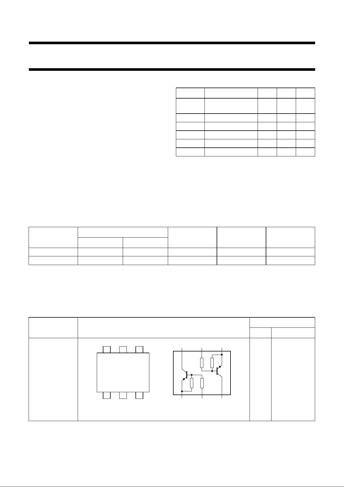
SIMPLIFIED OUTLINE, SYMBOL AND PINNING
PINNING
TYPE NUMBER SIMPLIFIED OUTLINE AND SYMBOL
PIN DESCRIPTION
PEMB13 1 emitter TR1
PUMB13 2 base TR1
46 5
654
R1 R2
TR1
R2
TR2
R1
3 collector TR2
4 emitter TR2
5 base TR2
6 collector TR1
123
Top view
MAM477
2004 Apr 15 2
123
Philips Semiconductors Product specification
PNP/PNP resistor-equipped transistors;
PEMB13; PUMB13
R1 = 4.7 kΩ, R2 = 47 kΩ
ORDERING INFORMATION
TYPE NUMBER
NAME DESCRIPTION VERSION
PEMB13 − plastic surface mounted package; 6 leads SOT666
PUMB13 − plastic surface mounted package; 6 leads SOT363
LIMITING VALUES
In accordance with the Absolute Maximum Rating System (IEC 60134).
SYMBOL PARAMETER CONDITIONS MIN. MAX. UNIT
Per transistor
V
V
V
V
CBO
CEO
EBO
I
collector-base voltage open emitter −−50 V
collector-emitter voltage open base −−50 V
emitter-base voltage open collector −−10 V
input voltage
positive − +5 V
negative −−30 V
I
I
P
O
CM
tot
output current (DC) −−100 mA
peak collector current −−100 mA
total power dissipation T
amb
SOT363 note 1 − 200 mW
SOT666 notes 1 and 2 − 200 mW
T
stg
T
j
T
amb
storage temperature −65 +150 °C
junction temperature − 150 °C
operating ambient temperature −65 +150 °C
Per device
P
tot
total power dissipation T
amb
SOT363 note 1 − 300 mW
SOT666 notes 1 and 2 − 300 mW
PACKAGE
≤ 25 °C
≤ 25 °C
Notes
1. Device mounted on an FR4 printed-circuit board, single-sided copper, standard footprint.
2. Reflow soldering is the only recommended soldering method.
2004 Apr 15 3
 Loading...