

Page 1

INTEGRATED CIRCUITS
PDIUSBH12
USB 2-port hub
Product specification
Supersedes data of 1999 Feb 25
1999 Jul 22
Page 2

Philips Semiconductors Product specification
PDIUSBH12USB 2-port hub
FEA TURES
•Complies with the Universal Serial Bus specification Rev. 1.0
•Complies with the ACPI, OnNOW, and USB power management
requirements
•Compliant with USB Human Interface Devices and Monitor
Control Class
•Compliant with System Management Bus Specification Rev. 1.0
•Two downstream ports with per packet connectivity and auto
speed detection
•Supports up to 3 embedded functions
•Integrated SIE (Serial Interface Engine), FIFO memory and
transceivers
•Automatic USB protocol handling
•High speed slave I
2
C Interface (up to 1 Mbit/s)
•Compatible with the PDIUSBH11 hardware and software
•Software controllable connection to USB bus (SoftConnect)
•Good USB downstream connection indicators that blink with traffic
(GoodLink)
•Low frequency 12 MHz crystal oscillator eases EMI design issues
•Programmable output clock frequency
•Bus powered capability with very low suspend current
•Controllable LazyClock output at 30 kHz (nominal) during suspend
•Single 3.3V supply with 5V tolerant I/O
•Available in 28-pin DIP and SO packages
•Full-scan design with high fault coverage (>99%) insures high
quality
•Higher than 8 KV in-circuit ESD protection lowers cost of extra
components
DESCRIPTION
The Universal Serial Bus Hub PDIUSBH12 is a cost and feature
optimized second generation USB Hub with 2 downstream ports and
3 embedded functions (compound hub). It is normally used in any
microcontroller-based system and communicates with the system
microcontroller over the high speed I
approach to implementing a hub and embedded functions allows the
designer to choose the optimum system microcontroller from the
available wide variety. This flexibility cuts down the development
time, risks and costs by allowing the use of the existing architecture
and the firmware investments. This results in the fastest way to
develop the most cost-effective USB peripheral solutions that need
hub functionality. The PDIUSBH12 is ideally suited for computer
monitors, docking stations, keyboards and many other applications
that use the I
The PDIUSBH12 conforms to the USB specification Rev 1.0, I2C
serial interface and the SMBus specifications. It is fully compliant
with the Human Interface Device Class and Monitor Control Class
specifications. Its low suspend power consumption along with the
programmable LazyClock output allows for easy implementation of
equipment that is compliant to the ACPI, OnNow and USB power
management requirements. The low operating power allows the
implementation of the bus powered or the compound powered hub
function.
The PDIUSBH12 is fully backward compatible to the first generation
PDIUSBH11 hardware and software. This allows an easy running
change in the manufacturing line to realize the cost savings. In
addition, it also incorporates the feature enhancements like
SoftConnect
lower frequency crystal oscillator, additional embedded functions
and integration of termination resistors. All of these feature
enhancements contribute to significant cost savings in the system
implementation and at the same time ease the implementation of
advanced USB functionality into the peripherals.
2
C or the SMBus based architecture.
, GoodLink, LazyClock, programmable clock output,
2
C serial bus. This modular
ORDERING INFORMATION
PACKAGES TEMPERATURE RANGE OUTSIDE NORTH AMERICA NORTH AMERICA PKG. DWG. #
28-pin plastic SO –40°C to +85°C PDIUSBH12 D PDIUSBH12 D SOT136-1
28-pin plastic DIP –40°C to +85°C PDIUSBH12 N PDIUSBH12 N SOT117-1
1999 Jul 22 853-2062 22025
2
Page 3
Philips Semiconductors Product specification
PDIUSBH12USB 2-port hub
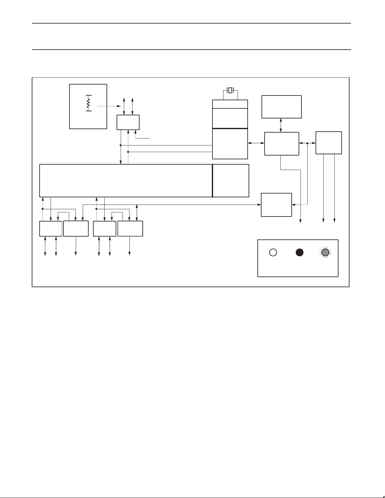
BLOCK DIAGRAM
UPSTREAM
3.3V
1.5kΩ
D+
SoftConnect
PORT
D+
ANALOG
TX/R
HUB
D–
X
FULL SPEED
REPEATER
ANALOG
T
X/RX
D–D+
DOWNSTREAM
PORT 2
GOODLINK
CONTROL
LED
ANALOG
T
X/RX
D–D+
DOWNSTREAM
PORT 3
GOODLINK
CONTROL
LED
NOTE:
1. This is a conceptual block diagram and does not include each individual signal.
12 MHz
PLL
BIT CLOCK
RECOVERY
PHILIPS
SIE
END OF
FRAME
TIMERS
INTEGRATED
RAM
MEMORY
MANAGEMENT
UNIT
GENERAL
PORT
CONTROLLER
INTERRUPT SDA SCL
NO LIGHT LIT BLINKING
NO
CONNECTION
CONNECTED
GOODLINK
I
SLAVE
INTERFACE
DATA
TRANSFER
SV00852
2
C
1999 Jul 22
3
Page 4

Philips Semiconductors Product specification
PDIUSBH12USB 2-port hub
Analog Transceivers
These transceivers interface directly to the USB cables through
some termination resistors. They are capable of transmitting and
receiving serial data at both “full speed” (12 Mbit/s) and “low speed”
(1.5 Mbit/s) data rates.
Hub Repeater
The hub repeater is responsible for managing connectivity on a per
packet basis. It implements packet signaling connectivity and
resume connectivity.
Low speed devices can be connected to downstream ports since the
repeater will not propagate upstream packets to downstream ports,
to which low speed devices are connected, unless they are
preceded by a PREAMBLE PID.
End of Frame Timers
This block contains the specified EOF1 and EOF2 timers which are
used to detect loss-of-activity and babble error conditions in the hub
repeater. The timers also maintain the low-speed keep-alive strobe
which is sent at the beginning of a frame.
General and Individual Port Controller
The general and individual port controllers together provide status
and control of individual downstream ports. Via the I
microcontroller can access the downstream ports and request or
change the status of each individual port.
Any change in the status or settings of the individual port will result
in an interrupt request. Via an interrupt register, the servicing
microcontroller can look up the downstream port which generated
the interrupt and request its new status. Any port status change can
then be reported to the host via the hub status change (interrupt)
endpoint.
2
C-interface a
PLL
A 12 MHz to 48 MHz clock multiplier PLL (Phase-Locked Loop) is
integrated on-chip. This allows for the use of low-cost 12 MHz
crystal. EMI is also minimized due to lower frequency crystal. No
external components are needed for the operation of the PLL.
Bit Clock Recovery
The bit clock recovery circuit recovers the clock from the incoming
USB data stream using 4X over-sampling principle. It is able to track
jitter and frequency drift specified by the USB specification.
Philips Serial Interface Engine (PSIE)
The Philips SIE implements the full USB protocol layer. It is
completely hardwired for speed and needs no firmware intervention.
The functions of this block include: synchronization pattern
recognition, parallel/serial conversion, bit stuffing/de-stuffing, CRC
checking/generation, PID verification/generation, address
recognition, handshake evaluation/generation.
Memory Management Unit (MMU) and Integrated RAM
The MMU and the integrated RAM is used to handle the large
difference in data rate between USB, running in bursts of 12 Mbit/s
and the I
1 Mbit/s. This allows the microcontroller to read and write USB
packets at its own speed through I2C.
2
C interface to the microcontroller, running at up to
I2C Slave Interface
This block implements the necessary I2C interface protocol. A slave
2
I
C allows for simple micro-coding. An interrupt is used to alert the
microcontroller whenever the PDIUSBH12 needs attention. As a
2
slave I
C device, the PDIUSBH12 I2C clock: SCL is an input and is
controlled by the microcontroller. The I
Mbit/s.
2
C interface can run up to 1
SoftConnect
The connection to the USB is accomplished by bringing D+ (for
high-speed USB device) high through a 1.5 kΩ pull-up resistor. In
the PDIUSBH12, the 1.5 kΩ pull-up resistor is integrated on-chip
and is not connected to V
pull-down resistors are integrated on-chip and are not connected to
GND by default. The connection of the internal resistors to Vcc is
established through a command sent by the external/system
microcontroller. This allows the system microcontroller to complete
its initialization sequence before deciding to establish connection to
the USB. Re-initialization of the USB bus connection can also be
affected without requiring the pull out of the cable.
The PDIUSBH12 will check for USB VBUS availability before the
connection can be established. VBUS sensing is provided through
OCURRENT_N pin. See the pin description for details. Sharing of
VBUS sensing and overcurrent sensing can be easily accomplished
by using VBUS voltage as the pull-up voltage for the open drain
output of the overcurrent indication device.
It should be noted that the tolerance of the internal resistors is
higher (30%) than that specified by the USB specification (5%).
However, the overall V
can still be met with good margin. The decision to make use of this
feature lies with the users.
SoftConnect is a patent pending technology from Philips
Semiconductors.
by default. Similarly, the 15 kΩ
CC
voltage specification for the connection
SE
GoodLink
Good downstream USB connection indication is provided through
GoodLink
least one valid upstream traffic from the port, the LED indicator will
be ON. The LED indicator will blink on every valid upstream traffic. A
valid upstream traffic is defined as traffic with a good SOP and
terminated by a good EOP. During global suspend, all LEDs will be
OFF.
This feature provides a user-friendly indicator on the status of the
hub, the connected downstream devices and the USB traffic. It is a
useful field diagnostics tool to isolate the faulty equipment. This
feature helps lower the field support and the hotline costs.
technology . When the port is enabled and there is at
1999 Jul 22
4
Page 5

Philips Semiconductors Product specification
01Control
2–3: Downstream
03Control
14Generic
1
27Generic
39Generic
01Control
2–3: Downstream
03Control
1
14Generic
011Control
6
17Generic
013Control
7
19Generic
PDIUSBH12USB 2-port hub
ENDPOINT DESCRIPTIONS
There are two endpoint configuration modes supported by the PDIUSBH12, the Single Embedded Function mode and the Multiple (3)
Embedded Function mode. The Single Embedded Function mode is the default at power up reset. The Multiple (3) Embedded Function mode
can be configured by writing a zero to bit 7 of the first byte of the Set Mode command. Either mode is backward compatible to the PDIUSBH11.
T able 1. SINGLE EMBEDDED FUNCTION MODE (DEFAULT AT POWER UP)
FUNCTION PORTS ENDPOINT #
Hub
Embedded
Function 1
NOTE:
1. Hub interrupt endpoint is not indexed.
2. Generic endpoint can be used for Interrupt or Bulk endpoint.
0: Upstream
ENDPOINT
INDEX
0
1
–
2
5
6
8
TRANSFER
TYPE
Interrupt
DIRECTION
OUT 8
IN 8
IN 1
OUT 8
IN 8
OUT 8
IN 8
OUT 8
IN 8
OUT 8
IN 8
MAX
PACKET SIZE
(BYTES)
T able 2. MULTIPLE (3) EMBEDDED FUNCTION MODE
FUNCTION PORTS ENDPOINT #
Hub
Embedded
Function 1
Embedded
Function 6
Embedded
Function 7
0: Upstream
1 – Interrupt IN 1
ENDPOINT
INDEX
0
2
5
10
6
12
8
TRANSFER
TYPE
DIRECTION
OUT 8
IN 8
OUT 8
IN 8
OUT 8
IN 8
OUT 8
IN 8
OUT 8
IN 8
OUT 8
IN 8
OUT 8
IN 8
MAX
PACKET SIZE
(BYTES)
1999 Jul 22
5
Page 6
Philips Semiconductors Product specification
PDIUSBH12USB 2-port hub
PINNING
The PDIUSBH12 has two modes of operation. The first mode (Mode 0) configures the pins DNx_GL_N for GoodLink LED indication. The
second mode (Mode 1) configures the LED pins as per port overcurrent condition pins. An overcurrent condition on any port can be uniquely
identified in Mode 1. However, all downstream ports are disabled as a result of a single overcurrent condition. In addition to the two modes of
operation, the PDIUSBH12 can also be configured to take either a 48 MHz crystal oscillator (for backward compatibility to PDIUSBH11) or a 12
MHz crystal.
The internal 4X clock multiplier PLL will be activated when 12 MHz input XTAL mode is selected. Also, the output clock frequenc y is now
programmable rather than fixed to 12 MHz. The output clock frequency can be programmed through the Set Mode command. All these new
features are added while maintaining backward compatibility to the PDIUSBH11 through TEST2 and TEST1 pins.
TEST2 TEST1
00
01
10
11
MODE
MODE 0
(GoodLink)
MODE 0
(GoodLink)
MODE 1
(Individual Overcurrent)
MODE 1
(Individual Overcurrent)
NOTE:
1. Pin TEST3 should always be connected to Ground at all times.
Pin configuration
1
2
TEST2
3
TEST3
RESET_N
CLKOUT
OCURRENT_N /
OCURRENT2_N
SWITCH_N
DN3_GL_N /
OCURRENT3_N
4
5
GND
6
XTAL1
7
XTAL2
8
9
V
CC
10
11
12 17
13 16 RSVDDN2_GL_N
14 15 RSVD
NOTE:
Pin 10 and Pin 14 show alternative pin functions, depending on
mode of operation (Mode 0 or Mode 1) as described in
Pin Description
.
28TEST1
27
26
25
24
23
22
21
20
19
18
UP_DM
UP_DP
AV
CC
AGND
DN2_DM
DN2_DP
DN3_DM
DN3_DP
GND
SCL
SDA
INT_NSUSPEND
SV01751
INPUT XTAL FREQUENCY
(MHz)
48 12MHz
12 4 MHz
12 4 MHz
48 12 MHz
OUTPUT CLOCK FREQUENCY
(AT REST)
1999 Jul 22
6
Page 7

Philips Semiconductors Product specification
PDIUSBH12USB 2-port hub
Pin description (MODE 0 – Good Link)
PIN NO. PIN SYMBOL TYPE DRIVE DESCRIPTION
1 TEST1 Input
2 TEST2 Input Connect to Ground
3 TEST3 Input Connect to Ground
4 RESET_N Input ST Power-on reset
5 GND Power Ground reference
6 XTAL1 Input Crystal connection 1 (48 or 12MHz depending on TEST1 pin)
7 XTAL2 Output Crystal connection 2 (48 or 12MHz depending on TEST1 pin)
8 CLKOUT Output 3mA Programmable output clock for external devices
9 V
10 OCURRENT_N Input ST
11 SWITCH_N Output OD6 Enables power to downstream ports
12 SUSPEND Output OD6 Device is in suspended state
13 DN2_GL_N Output OD6 Downstream port 2 GoodLink LED indicator
14 DN3_GL_N Output OD6 Downstream port 3 GoodLink LED indicator
15 RSVD Input Reserved. Connect to GND for normal operation.
16 RSVD Input Reserved. Connect to GND for normal operation.
17 INT_N Output OD6 Connect to microcontroller interrupt
18 SDA I/O OD6 I2C bi-directional data
19 SCL I/O OD6 I2C bit-clock
20 GND Power Ground reference
21 DN3_DP AI/O Downstream port 3 D+ connection
22 DN3_DM AI/O Downstream port 3 D– connection
23 DN2_DP AI/O Downstream port 2 D+ connection
24 DN2_DM AI/O Downstream port 2 D- connection
25 AGND Power Analog Ground reference
26 AV
27 UP_DP AI/O Upstream D+ connection
28 UP_DM AI/O Upstream D- connection
NOTE:
1. Signals ending in _N indicate active low signals.
ST: Schmitt Trigger
OD6: Open Drain with 6 mA drive
AI/O: Analog I/O
CC
CC
Power Voltage supply 3.3V ± 0.3V
Power Analog voltage supply 3.3V ± 0.3V
Connect to Ground for 48MHz crystal input.
Connect to VCC for 12MHz crystal input.
Over-current notice to the device. This pin is also used to sense the USB VBUS.
A LOW on this pin of less than 2 seconds is interpreted as an overcurrent notice;
longer than 2 seconds is interpreted as loss of VBUS.
1999 Jul 22
7
Page 8

Philips Semiconductors Product specification
PDIUSBH12USB 2-port hub
Pin description (MODE 1 – Individual Overcurrent)
PIN NO PIN SYMBOL TYPE DRIVE DESCRIPTION
1 TEST1 Input
2 TEST2 Input Connect to V
3 TEST3 Input Connect to Ground
4 RESET_N Input ST Power-on reset
5 GND Power Ground reference
6 XTAL1 Input Crystal connection 1 (48 or 12MHz depending on TEST1 pin)
7 XTAL2 Output Crystal connection 2 (48 or 12MHz depending on TEST1 pin)
8 CLKOUT Output 3mA Programmable output clock for external devices
9 V
10 OCURRENT2_N Input ST
11 SWITCH_N Output OD6 Enables power to downstream ports
12 SUSPEND Output OD6 Device is in suspended state
13 DN2_GL_N Output OD6 Downstream port 2 GoodLink LED indicator
14 OCURRENT3_N Input ST Downstream port 3 over-current notice
15 RSVD Input Reserved. Connect to GND for normal operation.
16 RSVD Input Reserved. Connect to GND for normal operation.
17 INT_N Output OD6 Connect to microcontroller interrupt
18 SDA I/O OD6 I2C bi-directional data
19 SCL I/O OD6 I2C bit-clock
20 GND Power Ground reference
21 DN3_DP AI/O Downstream port 3 D+ connection
22 DN3_DM AI/O Downstream port 3 D– connection
23 DN2_DP AI/O Downstream port 2 D+ connection
24 DN2_DM AI/O Downstream port 2 D- connection
25 AGND Power Analog Ground reference
26 AV
27 UP_DP AI/O Upstream D+ connection
28 UP_DM AI/O Upstream D- connection
NOTE:
1. Signals ending in _N indicate active low signals.
ST: Schmitt Trigger
OD6: Open Drain with 6 mA drive
AI/O: Analog I/O
CC
CC
Power Voltage supply 3.3V ± 0.3V
Power Analog voltage supply 3.3V ± 0.3V
Connect to VCC for 48MHz crystal input.
Connect to Ground for 12MHz crystal input.
CC
Downstream port 2 over-current notice. This pin is also use to sense the USB
VBUS. A LOW on this pin of less than 2 seconds is interpreted as an overcurrent
notice; longer than 2 seconds is interpreted as loss of VBUS.
1999 Jul 22
8
Page 9
Philips Semiconductors Product specification
PDIUSBH12USB 2-port hub
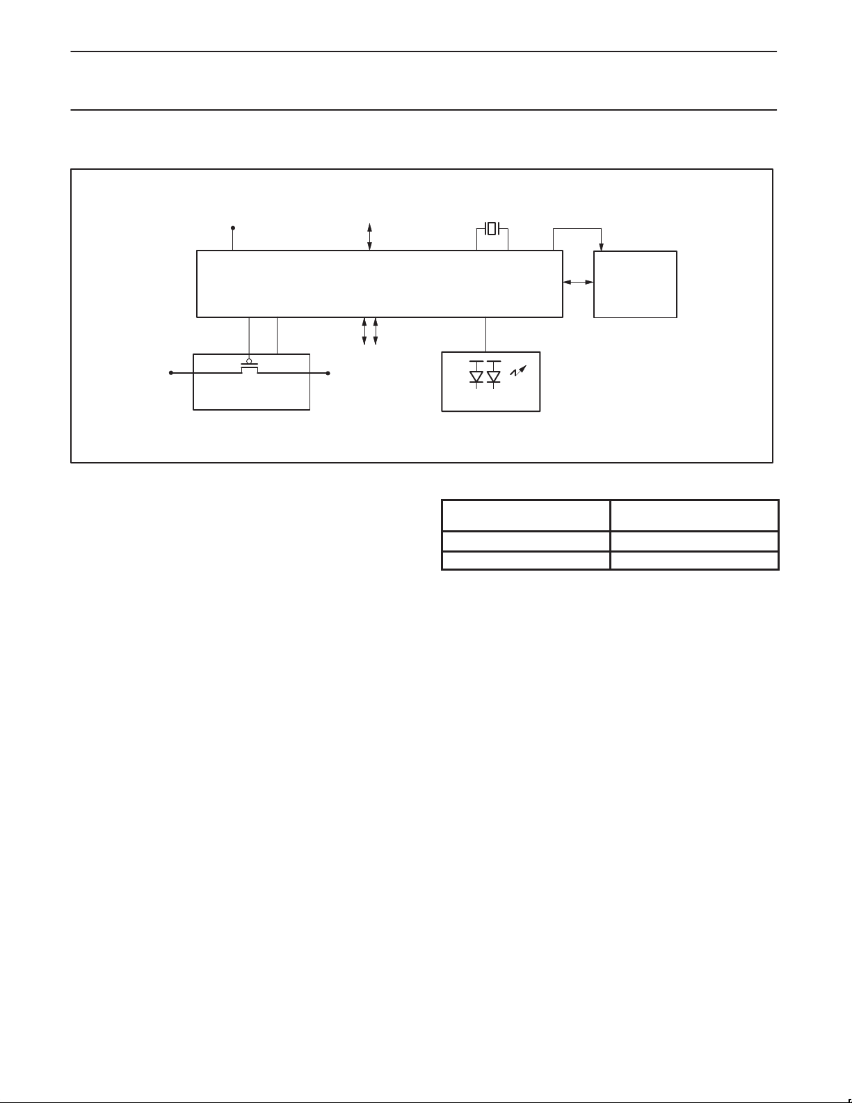
APPLICATION DIAGRAM
USB
3.3V
UPSTREAM
12MHz
CLKOUT
H12
USB
5V
POWER SWITCH
AND
OVERCURRENT CIRCUIT
DOWNSTREAM
SWITCHED
5V
I2C Interface
The I2C bus is used to interface to an external microcontroller
needed to control the operation of the hub. For cost consideration,
the target system microcontroller can be shared and utilized for this
purpose. The PDIUSBH12 implements a slave I
the PDIUSBH12 needs to communicate with the microcontroller it
asserts an interrupt signal. The microcontroller services this interrupt
by reading the appropriate status register on the PDIUSBH12
through the I
refer to the
2
C bus. (For more information about the I2C serial bus,
I2C Handbook
, Philips order number 9397 750 00013).
The I2C interface on the PDIUSBH12 defines two types of
transactions:
1. command transaction
A command transaction is used to define which data (e.g., status
byte, buffer data, ...) will be read from / written to the USB
interface in the next data transaction. A data transaction usually
follows a command transaction.
2. data transaction
A data transaction reads data from / writes data to the USB
interface. The meaning of the data is dependent on the
command transaction which was sent before the data
transaction.
Two addresses are used to differentiate between command and
data transactions. Writing to the command address is interpreted as
a command, while reading from / writing to the data address is used
to transfer data between the PDIUSBH12 and the controller.
2
C interface. When
I2C
GOODLINK LED
µC
SV00853
ADDRESS TABLE
TYPE OF ADDRESS
Command 0011 011 (binary)
Data 0011 010 (binary)
PHYSICAL ADDRESS
(MSB to LSB)
Protocol
An I2C transaction starts with a ‘Start Condition’, followed by an
address. When the address matches either the command or data
address the transaction starts and runs until a ‘Stop Condition’ or
another ‘Start Condition’ (repeated start) occurs.
The command address is write-only and is unable to do a read. The
next bytes in the message are interpreted as commands. Several
command bytes can be sent after one command address. Each of
the command bytes is acknowledged and passed on to the Memory
Management Unit inside the PDIUSBH12.
When the start condition address matches the data address, the
next bytes are interpreted as data. When the RW bit in the address
indicates a ‘master writes data to slave’ (=‘0’) the bytes are received,
acknowledged and passed on to the Memory Management Unit. If
the RW bit in the address indicates a ‘master reads data from slave’
(=‘1’) the PDIUSBH12 will send data to the master. The I
must acknowledge all data bytes except the last one. In this way the
2
I
C interface knows when the last byte has been transmitted and it
then releases the SDA line so that the master controller can
generate the STOP condition.
Repeated start support allows another packet to be sent without
generating a Stop Condition.
Timing
2
The I
C interface in the PDIUSBH12 can support clock speeds up to
1MHz.
2
C-master
1999 Jul 22
9
Page 10

Philips Semiconductors Product specification
PDIUSBH12USB 2-port hub
COMMAND SUMMARY
Some commands have the same command code (e.g., Read Buffer and Write Buffer). In these cases, the direction of the Data Phase (read or
write) indicates which command is executed.
COMMAND NAME
Set Address / Enable Hub D0h Write 1 byte
Set Endpoint Enable Hub + Embedded Functions D8h Write 1 byte
Set Mode Hub + Embedded Functions F3h Write 2 bytes
Read Interrupt Register F4h Read 2 bytes
Select Endpoint Hub Control OUT 00h Read 1 byte (optional)
Read Last Transaction Status Hub Control OUT 40h Read 1 byte
Read Endpoint Status Hub Control OUT 80h Read 1 byte
Read Buffer Selected Endpoint F0h Read n bytes
Write Buffer Selected Endpoint F0h Write n bytes
Set Endpoint Status Hub Control OUT 40h Write 1 byte
Acknowledge Setup Selected Endpoint F1h None
Clear Buffer Selected Endpoint F2h None
Validate Buf fer Selected Endpoint FAh None
Clear Port Feature Port 2 E0h Write 1 byte
Set Port Feature Port 2 E8h Write 1 byte
Get Port Status Port 2 E0h Read 1 or 2 bytes
Set Status Change Bits F7h Write 1 byte
Send Resume F6h None
Read Current Frame Number F5h Read 1 or 2 bytes
RECIPIENT CODING DATA PHASE
Initialization Commands
Embedded Function 1 D1h Write 1 byte
Embedded Function 6 D2h Write 1 byte
Embedded Function 7 D3h Write 1 byte
Data Flow Commands
Hub Control IN 01h Read 1 byte (optional)
Other Endpoints 00h + Endpoint Index Read 1 byte (optional)
Hub Control IN 41h Read 1 byte
Other Endpoints 40h + Endpoint Index Read 1 byte
Hub Control IN 81h Read 1 byte
Other Endpoints 80h + Endpoint Index Read 1 byte
Hub Control IN 41h Write 1 byte
Other Endpoints 40h + Endpoint Index Write 1 byte
Hub Commands
Port 3 E1h Write 1 byte
Port 3 E9h Write 1 byte
Port 3 E1h Read 1 or 2 bytes
General Commands
1999 Jul 22
10
Page 11

Philips Semiconductors Product specification
PDIUSBH12USB 2-port hub
COMMAND DESCRIPTIONS
Command Procedure
There are four basic types of commands: Initialization, Data, Hub
Specific, and General commands. Respectively, these are used to
initialize the hub and embedded function; for data flow between the
hub, embedded function, and the host; some hub specific
commands for controlling individual downstream ports; and some
general commands.
Initialization Commands
Initialization commands are used during the enumeration process of
the USB network. These commands are used to enable the hub and
embedded function endpoints. They are also used to set the USB
assigned address.
Set Address / Enable
Command : D0h (Hub), D1h, D2h, D3h,
Data : Write 1 byte
This command is used to set the USB assigned address and enable
the hub or embedded functions respectively. The hub powers up
enabled and needs not be enabled by the firmware at power up
initialization.
(Embedded Functions)
7654320100
000000
POWER ON VALUE
ADDRESS
ENABLE
SV00825
Set Endpoint Enable
Command : D8h
Data : Write 1 byte
The hub’s interrupt endpoint and the embedded functions generic
endpoints can only be enabled when the corresponding hub/function
is enabled via the Set Address/Enable command.
7654320100
00XXXX
Hub’s Interrupt Endpoint A value of ‘1’ indicates
Embedded Function 1 Generic Endpoint A value of ‘1’ indicates
Embedded Function 6 Generic Endpoint A value of ‘1’ indicates
Embedded Function 7 Generic Endpoint A value of ‘1’ indicates
POWER ON VALUE
HUB’S INTERRUPT ENDPOINT
EMBEDDED FUNCTION 1 GENERIC ENDPOINTS
EMBEDDED FUNCTION 6 GENERIC ENDPOINTS
EMBEDDED FUNCTION 7 GENERIC ENDPOINTS
RESERVED
SV00841
the hub’s interrupt
endpoint is enabled.
the embedded function
1 generic endpoints are
enabled.
the embedded function
6 generic endpoints are
enabled.
the embedded function
7 generic endpoints are
enabled.
Address The value written becomes the address.
Enable A ‘1’ enables this function.
1999 Jul 22
Set Mode
Command : F3h
Data : Write 2 bytes
The Set Mode command is followed by two data writes. The first
byte contains the configuration byte values. The second byte is the
clock division factor byte.
11
Page 12

Philips Semiconductors Product specification
PDIUSBH12USB 2-port hub
Configuration Byte
7654320110
Remote Wakeup A ‘1’ indicates that a remote
No LazyClock A ‘1’ indicates that CLKOUT will
Clock Running A ‘1’ indicates that the internal
Debug Mode A ‘1’ indicates that all errors and
SoftConnect A ‘1’ indicates that the upstream
110010
POWER ON VALUE
REMOTE WAKEUP
NO LAZYCLOCK
CLOCK RUNNING
DEBUG MODE
SoftConnect
CONNECT DOWNSTREAM RESISTORS
NON-BLINKING LEDs
EMBEDDED FUNCTION MODE
SV00842
wakeup feature is ON. Bus reset
will set this bit to ‘1’.
not switch to LazyClock. A ‘0’
indicates that the CLKOUT
switches to LazyClock 1ms after
the Suspend pin goes high.
LazyClock frequency is 30KHz (±
40%). The programmed value will
not be changed by a bus reset.
clocks and PLL are always
running even during Suspend
state. A ‘0’ indicates that the
internal clock, crystal oscillator
and PLL are stopped whenever
not needed. To meet the strict
Suspend current requirement, this
bit needs to be set to ‘0’. The
programmed value will not be
changed by a bus reset.
“NAKing” are reported and a ‘0’
indicates that only OK and
babbling are reported. The
programmed value will not be
changed by a bus reset.
pull-up resistor will be connected if
VBUS is available. A ‘0’ means
that the upstream resistor will not
be connected. The programmed
value will not be changed by a bus
reset.
Connect Downstream Resistors A ‘1’ indicates that downstream
resistors are connected. A ‘0’
means that downstream resistors
are not connected. The
programmed value will not be
changed by a bus reset.
Non-blinking LEDs A ‘1’ indicates that GoodLink
LEDs will NOT blink when there is
traffic. Leave this bit at ‘0’ to
achieve blinking LEDs. The
programmed value will not be
changed by a bus reset.
Embedded Function Mode A ‘1’ indicates single embedded
function mode. A ‘0’ indicates
multiple (3) embedded function
mode. See
endpoint descriptions
for details. The programmed value
will not be changed by a bus
reset.
Clock Division Factor Byte
7654321110
0000XX
111011XX
Clock Division Factor The value indicates clock division
POWER ON VALUE FOR 48MHz INPUT
POWER ON VALUE FOR 12MHz INPUT
CLOCK DIVISION FACTOR
RESERVED
SV00843
factor for CLKOUT. The output
frequency is 48 MHz/(N+1) where
N is the Clock Division Factor. The
reset value is 3. This will give a
default output frequency at
CLKOUT pin of 12 MHz, thus
maintaining backward
compatibility to the PDIUSBH11.
When the 12 MHz input crystal
frequency is selected, the reset
value is 11. This will produce the
lowest output frequency of 4 MHz
which can then be programmed
up by the user. The PDIUSBH12
design ensures no glitching during
frequency change. The
programmed value will not be
changed by a bus reset.
1999 Jul 22
12
Page 13

Philips Semiconductors Product specification
PDIUSBH12USB 2-port hub
Data Flow Commands
Data flow commands are used to manage the data transmission
between the USB endpoints and the monitor. Much of the data flow
is initiated via an interrupt to the microcontroller. The microcontroller
utilizes these commands to access and determine whether the
endpoint FIFOs have valid data.
Read Interrupt Register
Command : F4h
Data : Read 2 bytes
Interrupt Register Byte 1
7654320100
Interrupt Register Byte 2
7654320100
This command indicates the origin of an interrupt. A ‘1’ indicates an
interrupt occurred at this endpoint. The bits are cleared by reading
the endpoint status register through Read Endpoint Status
command.
After a bus reset an interrupt will be generated and bit 6 of the
Interrupt Register Byte 2 will be ‘1’. [In the PDIUSBH11, the bus
reset event is indicated by the absence of a ‘1’ in any bit of the
Interrupt Register. Note that the backward compatibility is still
maintained because in the PDIUSBH11, the Interrupt Register Byte
2 does not exist.]
The bus reset interrupt is internally cleared by reading the interrupt
register. A bus reset is completely identical to the hardware reset
through the RESET_N pin with the sole difference of interrupt
notification.
The hub interrupt endpoint is handled internally by the PDIUSBH12
hardware without the need of microcontroller intervention.
000000
0000X0
POWER ON VALUE
ENDPOINT INDEX 0 (HUB CONTROL OUT)
ENDPOINT INDEX 1 (HUB CONTROL IN)
ENDPOINT INDEX 2
ENDPOINT INDEX 3
ENDPOINT INDEX 4
ENDPOINT INDEX 5
ENDPOINT INDEX 6
ENDPOINT INDEX 7
SV00844
POWER ON VALUE
ENDPOINT INDEX 8
ENDPOINT INDEX 9
ENDPOINT INDEX 10
ENDPOINT INDEX 11
ENDPOINT INDEX 12
ENDPOINT INDEX 13
BUS RESET
RESERVED
SV00845
Select Endpoint
Command : 00-0Dh
Data : Optional Read 1 byte
The Select Endpoint command initializes an internal pointer to the
start of the Selected buffer. Optionally, this command can be
followed by a data read, which returns ‘0’ if the buffer is empty and
‘1’ if the buffer is full.
765432X100
XXXXXX
POWER ON VALUE
FULL/EMPTY
RESERVED
SV00831
Full/Empty A ‘1’ indicates the buffer is full, ‘0’
indicates an empty buffer.
Read Last Transaction Status
Command : 40–4Dh
Data : Read 1 byte
The Read Last Transaction Status command is followed by one data
read that returns the status of the last transaction of the endpoint.
This command also resets the corresponding interrupt flag in the
interrupt register, and clears the status, indicating that it was read.
This command is useful for debugging purposes. Since it keeps
track of every transaction, the status information is overwritten for
each new transaction.
7654320100
Data Receive/Transmit Success A ‘1’ indicates data has been
Error Code See Table 3, Error Codes.
Setup Packet A ‘1’ indicates the last
Data 0/1 Packet A ‘1’ indicates the last
Previous Status not Read A ‘1’ indicates a second event
000000
POWER ON VALUE
DATA RECEIVE/TRANSMIT SUCCESS
ERROR CODE (SEE TABLE)
SETUP PACKET
DATA 0/1 PACKET
PREVIOUS STATUS NOT READ
SV00832
received or transmitted
successfully.
successful received packet
had a SETUP token (this will
always read ‘0’ for IN buffers.
successful received or sent
packet had a DATA1 PID.
occurred before the previous
status was read.
1999 Jul 22
13
Page 14

Philips Semiconductors Product specification
PDIUSBH12USB 2-port hub
Table 3. Error codes
ERROR
CODE
0000 No Error
0001
0010
0011
0100 Token CRC Error
0101 Data CRC Error
0110 Time Out Error
0111 Babble Error
1000 Unexpected End-of-packet
1001 Sent or received NAK
1010
1011
1101 Bitstuff Error
1111
PID encoding Error; bits 7–4 are not the inversion of
bits 3–0
PID unknown; encoding is valid, but PID does not
exist
Unexpected packet; packet is not of the type expected
(= token, data or acknowledge), or SETUP token to a
non-control endpoint
Sent Stall, a token was received, but the endpoint was
stalled
Overflow Error, the received packet was longer than
the available buffer space
Wrong DATA PID; the received DATA PID was not the
expected one
RESULT
Read Endpoint Status
Command : 80–8Dh
Data : Read 1 byte
765432X1X0
Setup Packet A ‘1’ indicates the last received
STALL A ‘1’ indicates the endpoint is
Data 0/1 Packet A ‘1’ indicates if the last received
Buffer Full A ‘1’ indicates that the buffer is
0000XX
POWER ON VALUE
RESERVED
SETUP PACKET
STALL
DATA 0/1 PACKET
BUFFER FULL
RESERVED
SV00833
packet had a SETUP token.
stalled.
or sent packet had a DATA1 PID.
full.
Read Buffer
Command : F0h
Data : Read multiple bytes (max 10)
The Read Buffer command is followed by a number of data reads,
which return the contents of the selected endpoint data buffer. After
each read, the internal buffer pointer is incremented by 1.
The buffer pointer is not reset to the buffer start by the Read Buffer
command. This means that reading or writing a buffer can be
interrupted by any other command (except for Select Endpoint), or
can be done by more than one I
to get the number of data bytes, then read the rest in other
transactions).
The data in the buffer are organized as follows:
2
C transaction (read the first 2 bytes
•byte 0: Reserved: can have any value
•byte 1: Number/length of data bytes
•byte 2: Data byte 1
•byte 3: Data byte 2
Write Buffer
Command : F0h
Data : Write multiple bytes (max 10)
The Write Buffer command is followed by a number of data writes,
which load the endpoints buffer. The data must be organized in the
same way as described in the Read Buffer command. The first byte
(reserved) should always be 0. As in the Read Buffer command, the
data can be split up into different I
WARNING:
There is no protection against writing or reading over a buffer’s
boundary or against writing into an OUT buffer or reading from an IN
buffer . Any of these actions could cause an incorrect operation. Data
in an OUT buffer are only meaningful after a successful transaction.
Clear Buffer
Command : F2h
Data : None
When a packet is received completely, an internal endpoint buffer
full flag is set. All subsequent packets will be refused by returning a
NAK. When the microcontroller has read the data, it should free the
buffer by the Clear Buffer command. When the buffer is cleared new
packets will be accepted.
Validate Buffer
Command : FAh
Data : None
When the microprocessor has written data into an IN buffer, it should
set the buffer full flag by the Validate Buffer command. This indicates
that the data in the buffer are valid and can be sent to the host when
the next IN token is received.
2
C data transactions.
1999 Jul 22
14
Page 15

Philips Semiconductors Product specification
PDIUSBH12USB 2-port hub
Set Endpoint Status
Command : 40–4Dh
Data : Write 1 byte
A stalled control endpoint is automatically unstalled when it receives
a SETUP token, regardless of the content of the packet. If the
endpoint should stay in its stalled state, the microcontroller can
re-stall it.
When a stalled endpoint is unstalled (either by the Set Endpoint
Status command or by receiving a SETUP token), it is also
re-initialized. This flushes the buffer and if it is an OUT buffer it waits
for a DATA 0 PID, if it is an IN buffer it writes a DATA 0 PID.
Even when unstalled, writing Set Endpoint Status to ‘0’ initializes the
endpoint.
765432X100
Stalled A ‘1’ indicates the endpoint is stalled.
XXXXXX
POWER ON VALUE
STALLED
RESERVED
SV00834
Acknowledge Setup
Command : F1h
Data : None
The arrival of a SETUP packet flushes the IN buffer and disables the
Validate Buffer and Clear Buffer commands for both IN and OUT
endpoints.
The microcontroller needs to re-enable these commands by the
Acknowledge Setup command. This ensures that the last SETUP
packet stays in the buffer and no packet can be sent back to the
host until the microcontroller has acknowledged explicitly that it has
seen the SETUP packet.
The microcontroller must send the Acknowledge Setup command to
both the IN and OUT endpoints.
Hub Commands
Hub commands are used to report connectivity and power status
between the hub and the host. These commands allow the host to
enable each port individually and get any change of status such as
new connectivity information.
Clear/Set Port Feature
Command : E0–E1h (Clear) and E8h–E9h (Set)
Data : Write 1 byte
The data written in the data phase is the feature code described in
Table 4.
When the controller receives a Set Feature or a Clear Feature
request, there are two possibilities:
The request applies to port 1, the embedded port. In this case the
request should be handled internally by the controller.
If the request applies to ports 2 and 3, the controller should translate
the request into a Set Feature or Clear Feature command towards
the PDIUSBH12.
When the PDIUSBH12 is configured in mode 0, there is only one
power switch output and one overcurrent input. This means that the
F_PORT_POWER and C_PORT_OVERCURRENT features are not
port specific. For these features, any of the Set / Clear Feature
commands can be used. The specific port assignment is ignored.
When the PDIUSBH12 is configured in mode 1, there is still only one
power switch output but there are two individual overcurrent input
pins corresponding to each port. This means that the
F_PORT_POWER feature is port specific and the
C_PORT_OVERCURRENT feature is not port specific.
Setting the F_PORT_POWER feature turns the power on when it is
off and turns the overcurrent detection on only when the power is
already on. This allows it to have a short period of overcurrent
condition at the moment that power is switched on. For this reason,
the F_PORT_POWER feature needs to be set twice. Clearing this
feature turns both the power and the overcurrent detection off.
Table 4.
FEATURE FEATURE CODE SET CLEAR
F_PORT_ENABLE 0 Enables a port Disables a port
F_PORT_SUSPEND 1 Suspends a port Resumes a port
FC_PORT_RESET 2 Resets a port Clears a port Reset Change bit
F_PORT_POWER 3 Powers all ports Unpowers all ports
C_PORT_CONNECTION 4 – Clears a port Connection Change bit
C_PORT_ENABLE 5 – Clears a port Enable Change bit
C_PORT_SUSPEND 6 – Clears a port Suspend Change bit
C_PORT_OVERCURRENT 7 – Clears a port (Mode 1) or hub (Mode 0) Overcurrent Change bit
1999 Jul 22
15
Page 16

Philips Semiconductors Product specification
PDIUSBH12USB 2-port hub
Get Port Status
Command : E0h–E1h
Data : Read 1 or 2 bytes
The Get Port Status Command can be followed by one or two data
reads. The first byte returned contains the port status. The second
byte returned is the port status change byte.
Port Status Byte
7654320100
Connect A ‘1’ indicates that a device is connected on
Enabled A ‘1’ indicates that this port is enabled.
Suspend A ‘1’ indicates that this port is suspended.
OverCurrent A ‘1’ indicates that overcurrent condition
Reset A ‘1’ indicates that bus reset on this port is in
Power A ‘1’ indicates that power is supplied to
Low Speed A ‘1’ indicates that low speed device is
0000X0
POWER ON VALUE
CONNECT
ENABLED
SUSPEND
OVERCURRENT
RESET
POWER
LOW SPEED
RESERVED
SV00846
this port of the hub.
exists on this port. In mode 0 of operation,
this bit is the same for all ports. In mode 1,
individual port overcurrent indication is
possible.
progress. When reset is completed (nominal
duration of 10 ms), this bit indicates a ‘0’.
downstream ports. Since the PDIUSBH12
supports gang mode power switching, this
bit is the same for all ports.
connected to this port. This bit is only valid
when Connect bit is a ‘1’.
Port Status Change Byte
The description for the Port Status Change Byte is similar to the Port
Status Byte except that the value of the bits are ‘1’ only when a
change has occurred.
7654320100
00X0XX
POWER ON VALUE
CONNECT
ENABLED
SUSPEND
OVERCURRENT
RESET
RESERVED
SV00847
Set Status Change Bits
Command : F7h
Data : Write 1 byte
For assembling the hub’s status change register, the device needs
some additional information from the controller, i.e. the Local Power
Status Change bit and the embedded function Status Change bit.
These are provided by the Set Status Change Bits command. This
command is always followed by one data write which contains the
Local Power Status Change bit at the LSB and the embedded
function Status Change bit at position 1. All other bits should be 0.
7654320100
00XXXX
POWER ON VALUE
LOCAL POWER
EMBEDDED FUNCTION 1
EMBEDDED FUNCTION 6
EMBEDDED FUNCTION 7
RESERVED
SV00848
1999 Jul 22
16
Page 17

Philips Semiconductors Product specification
PDIUSBH12USB 2-port hub
General Commands
Send Resume
Command : F6h
Data : None
Sends an upstream resume signal for 10 ms. This command is
normally issued when the device is in suspend. The RESUME
command is not followed by a data read or write.
The PDIUSBH12 automatically sends a RESUME command when
an event occurs downstream.
Read Current Frame Number
Command : F5h
Data : Read One or Two Bytes
This command is followed by one or two data reads and returns the
frame number of the last successfully received SOF. The frame
number is returned Least Significant Byte first.
765432X1X0
765432X1X0
XXXXXX
XXXXXX
LEAST SIGNIFICANT BYTE
MOST SIGNIFICANT BYTE
SV00835
Embedded Function
The USB host sees no difference between the embedded function
and a function connected to one of the downstream ports. Some of
the port commands sent by the host must be handled appropriately
by the embedded function to appear as any other downstream port.
The microcontroller maintains a series of status and status change
bits for the embedded function as described in the Get Port Status
command section. From these bits, the Status Change bit for the
embedded function is derived (i.e. the port specific Status Change
bits). This Status Change bit is then provided to the PDIUSBH12 by
the Set Status Change Bits command.
Host Requests
SetFeature PORT_RESET
Reinitialize the embedded function and set the Reset Change bit to
indicate that the reset has completed. Reset the Enable Status bit,
enable the embedded function and set its address to ‘0’ by the Set
embedded function Address / Enable command. Disable the
embedded function interrupt endpoint by the Set Endpoint Enable
command.
SetFeature PORT_ENABLE
Enable the function by the Set embedded function Address/Enable
command. Set the Enable Status bit.
SetFeature PORT_SUSPEND
Disable the function by the Set embedded function Address/Enable
command. Reset the Enable Status bit and set the Suspend Status
bit.
ClearFeature PORT_ENABLE
Disable the function by the Set embedded function Address / Enable
command. Reset the Enable Status bit.
ClearFeature PORT_SUSPEND
Enable the function by the Set embedded function Address / Enable
command. Set the Enable Status bit, reset the Suspend Status bit;
set the Resume Status Change bit to indicate that the resume has
completed.
ClearFeature any Change Indicator
Clear the corresponding status change bit.
Babbling condition
When the embedded function causes a babbling condition, the
function is automatically disabled by the PDIUSBH12. As soon as
the microcontroller detects the babbling error, it must set the Enable
Status Change bit and reset the Enable Status bit.
Remote WakeUp
There are three scenarios when a remote wakeup can occur. The
following describes the course of actions for each of the cases:
1. The device is not suspended and the embedded port is
suspended:
Enable back the function by setting the enable bit in the Set
Address/Enable register and update the following status bits in
the microcontroller program: reset the Suspend Status bit, set
the Enable Status bit and set the Suspend Status Change bit.
2. The device is suspended and the embedded port is suspended:
Send an upstream Resume using the Send Resume command,
enable back the function by setting the enable bit in the Set
Address/Enable register and update the following status bits in
the microcontroller program: reset the Suspend Status bit, set
the Enable Status bit and set the Suspend Status Change bit.
3. The device is suspended and the embedded port is enabled:
Send an upstream resume using the Send Resume command.
1999 Jul 22
17
Page 18

Philips Semiconductors Product specification
PDIUSBH12USB 2-port hub
RECOMMENDED OPERATING CONDITIONS
SYMBOL PARAMETER TEST CONDITIONS MIN MAX UNIT
V
T
V
V
V
CC
V
AI/O
amb
DC supply voltage 3.0 3.6 V
DC input voltage range 0 5.5 V
I
DC input voltage range for I/O 0 5.5 V
I/O
DC input voltage range for analog I/O 0 V
DC output voltage range 0 V
O
Operating ambient temperature range in free air See DC and AC characteristics per device –40 85 °C
CC
CC
V
V
ABSOLUTE MAXIMUM RATINGS
SYMBOL
I
GND
V
CC
I
IK
V
I
V
I/O
I
OK
V
O
I
O
I
O
, I
V
ESD
T
STG
P
TOT
DC supply voltage –0.5 +4.6 V
DC input diode current VI < 0 –50 mA
DC input voltage Note 2 –0.5 +5.5 V
DC input voltage range for I/O’s –0.5 VCC + 0.5 V
DC output diode current VO > VCC or VO < 0 ±50 mA
DC output voltage Note 2 –0.5 VCC + 0.5 V
DC output sink or source current for other pins VO = 0 to V
DC output sink or source current for D+/D– pins VO = 0 to V
DC VCC or GND current ±100 mA
CC
Electrostatic discharge voltage IIL < 1 µA
Storage temperature range –60 +150 °C
Power dissipation per package
1
PARAMETER TEST CONDITIONS MIN MAX UNIT
CC
CC
3
— ±4000
±15 mA
±50 mA
4
V
NOTES:
1. Stresses beyond those listed may cause damage to the device. These are stress ratings only and functional operation of the device at these
or any other conditions beyond those listed in the RECOMMENDED OPERATING CONDITIONS table is not implied. Exposure to absolute
maximum rated conditions for extended periods may affect device reliability .
2. The input and output voltage ratings may be exceeded if the input and output current ratings are observed.
3. Values are given for device only: in-circuit V
4. For open-drain pins V
ESD(MAX)
= ±2000 V .
ESD(MAX)
= ±8000 V .
1999 Jul 22
18
Page 19

Philips Semiconductors Product specification
VOLLOW level out ut voltage
VOHHIGH level out ut voltage
PDIUSBH12USB 2-port hub
DC CHARACTERISTICS (Digital pins)
SYMBOL PARAMETER TEST CONDITIONS MIN TYP MAX UNIT
Input Levels
V
VIH
V
TLH
V
THL
V
HYS
Output Levels
Leakage Current
I
OZ
I
I
I
LOW level input voltage 0.6 V
IL
HIGH level input voltage 2.7 V
LOW to HIGH threshold voltage ST (Schmitt Trigger) pins 1.4 1.9 V
HIGH to LOW threshold voltage ST pins 0.9 1.5 V
Hysteresis voltage ST pins 0.4 0.7 V
p
p
IOL = rated drive 0.4
IOL = 20 µA 0.1 V
IOH = rated drive 2.4
IOH = 20 µA VCC – 0.1 V
OFF state current OD (Open Drain) pins ±1 µA
Input leakage current ±1 µA
L
Suspend current
S
Operating current 02 ports operating 13 mA
O
Oscillator stopped and
inputs to GND/V
CC
V
V
15 µA
DC CHARACTERISTICS (AI/O pins)
SYMBOL PARAMETER TEST CONDITIONS MIN MAX UNIT
Leakage Current
I
LO
Hi-Z state data line leakage 0V < VIN < 3.3V ±10 µA
Input Levels
V
V
CM
V
Differential input sensitivity |(D+) – (D–)|
DI
Differential common mode range Includes VDI range 0.8 2.5 V
Single-ended receiver threshold 0.8 2.0 V
SE
1
0.2 V
Output Levels
V
V
OH
Static output LOW RL of 1.5kΩ to 3.6V 0.3 V
OL
Static output HIGH RL of 15kΩ to GND 2.8 3.6 V
Capacitance
C
Transceiver capacitance Pin to GND 20 pF
IN
Output Resistance
2
Z
DRV
Driver output resistance Steady state drive 28 43 Ω
Integrated Resistance
Z
PU
Z
PD
Pull-up resistance SoftConnect = ON 1.1 1.9 kΩ
Pull-down resistance Pull-down = ON 11 19 kΩ
NOTES:
1. D+ is the symbol for the USB positive data pin: UP_DP, DN2_DP, DN3_DP.
D– is the symbol for the USB negative data pin: UP_DM, DN2_DM, DN3_DM.
2. Includes external resistors of 22 W ± 1% each on D+ and D–.
LOAD FOR D+/D–
1.5kΩ IS INTERNAL
TEST POINT
D. U. T .
22Ω
15kΩ
C
L
= 50pF
1999 Jul 22
SV00849
19
Page 20

Philips Semiconductors Product specification
Between 10% and 90%
PDIUSBH12USB 2-port hub
AC CHARACTERISTICS (AI/O pins, FULL speed)
SYMBOL PARAMETER TEST CONDITIONS MIN MAX UNIT
Driver characteristics CL = 50pF;
Transition Time:
t
V
t
r
t
RFM
CRS
f
Rise time
Fall time
Rise/fall time matching (tr/tf) 90 110 %
Output signal crossover voltage 1.3 2.0 V
Driver Timings
t
EOPT
t
DEOP
Source EOP width Figure 1 160 175 ns
Differential data to EOP transition skew Figure 1 –2 5 ns
Receiver Timings
Receiver Data Jitter Tolerance
t
t
JR1
JR2
To next transition
For paired transitions
EOP Width at Receiver
t
EOPR1
t
EOPR2
Must reject as EOP Figure 1 40 ns
Must accept 82 ns
Hub Timings Full Speed downstream port.
t
HDD
t
SOP
t
EOPDR
t
HESK
Hub Differential Data Delay Figure 2 40 ns
Data bit width distortion after SOP Figure 2 –5 3 ns
Hub EOP Delay Relative to t
HDD
Hub EOP Output Width Skew Figure 3 –15 +15 ns
Rpu = 1.5kΩ on D+ to V
CC
4 20 ns
4 20 ns
Characterized and not tested.
Guaranteed by design.
–18.5 18.5 ns
–9 9 ns
Figure 3 0 15 ns
1999 Jul 22
20
Page 21

Philips Semiconductors Product specification
t
Rise time
t
Fall time
Figure 1
PDIUSBH12USB 2-port hub
AC CHARACTERISTICS (AI/O pins, LOW speed)
SYMBOL PARAMETER TEST CONDITIONS MIN MAX UNIT
Driver characteristics
Transition Time Between 10% and 90%
lr
lf
t
V
RFM
LCRS
Rise/fall time matching (tr/tf) 80 120 %
Output signal crossover voltage 1.3 2.0 V
Driver Timings
t
LEOPT
t
LDEOP
Source EOP width Figure 1 1.25 1.50 µs
Differential data to EOP transition skew Figure 1 –40 100 ns
Receiver Timings
EOP Width at Receiver
t
LEOPR1
t
LEOPR2
Must reject as EOP
Must accept
Hub Timings Low Speed downstream port.
t
LHDD
t
LSOP
t
LEOPDR
t
LHESK
Hub Differential Data Delay Figure 2 300 ns
Data bit width distortion after SOP Figure 2 –65 45 ns
Hub EOP Delay Relative to T
HDD
Hub EOP Output Width Skew Figure 3 –300 +300 ns
CL = 50pF and 350pF;
Rpu = 1.5kΩ on D– to V
CC
CL = 50pF 75 ns
CL = 350pF 300 ns
CL = 50pF 75 ns
CL = 350pF 300 ns
330 ns
675 ns
Figure 3 0 200 ns
t
PERIOD
DIFFERENTIAL
DATA LINES
CROSSOVER POINT
CROSSOVER POINT
DIFFERENTIAL DATA TO
SEO/EOP SKEW
N * t
PERIOD
+ t
DEOP
EXTENDED
SOURCE EOP WIDTH: t
RECEIVER EOP WIDTH: t
Figure 1. Differential data to EOP transition skew and EOP width
EOPT
EOPR1
, t
EOPR2
SV00837
1999 Jul 22
21
Page 22

Philips Semiconductors Product specification
PDIUSBH12USB 2-port hub
V
DD
UPSTREAMDIFFERENTIAL
DATA
V
SS
DOWNSTREAMDIFFERENTIAL
DATA
V
SS
A. DOWNSTREAM HUB DELAY B. UPSTREAM HUB DELAY
SOP DISTORTION
= t
t
SOP
HDD
LOW SPEED TIMINGS ARE DETERMINED IN THE SAME WAY FOR:
t
AND t
LHDD
(SOP) – t
LSOP
CROSSOVER
POINT
Hub Delay
Downstream
t
(NEXT J)
HDD
HDD
CROSSOVER
POINT
DOWNSTREAM
DIFFERENTIAL
DATA
UPSTREAM
DIFFERENTIAL
DATA
Figure 2. Hub Differential Data Delay and SOP distortion
CROSSOVER
POINT
Hub Delay
Upstream
t
HDD
CROSSOVER
POINT
SV00514
V
DD
UPSTREAMDIFFERENTIAL
DATA
V
SS
DOWNSTREAMDIFFERENTIAL
DATA
V
SS
DOWNSTREAM
PORT
UPSTREAM
END OF CABLE
t
EOP–
t
EOP–
t
EOP+
CROSSOVER
POINT
EXTENDED
CROSSOVER
POINT
EXTENDED
A. DOWNSTREAM EOP DELAY B. UPSTREAM EOP DELAY
EOP DELAY
= t
t
EOPD
EOP–
EOP DELAY RELATIVE TO t
t
= t
= t
, t
EOPD
EOP+
LEOPDR
– t
– t
EOP–
, AND t
EOPDR
EOP SKEW
t
HESK
LOW SPEED TIMINGS ARE DETERMINED IN THE SAME WAY FOR:
t
LEOPD
HDD
HDD
LHESK
Figure 3. Hub EOP Delay and EOP Skew
t
EOP+
CROSSOVER
POINT
EXTENDED
CROSSOVER
POINT
EXTENDED
SV00515
1999 Jul 22
22
Page 23

Philips Semiconductors Product specification
PDIUSBH12USB 2-port hub
AC CHARACTERISTICS (I2C pins)
All timing values are valid within the operating supply voltage and ambient temperature range and reference to VIL and VIH with an input voltage
swing of V
SYMBOL
t
t
t
t
t
t
SU;STO
A detailed description of the I2C-bus specification, with applications, is given in the brochure “
be ordered using the Philips order number 9398 393 40011.
f
SCL
t
BUF
SU;STA
HD;STA
t
LOW
t
HIGH
t
r
t
f
SU;DAT
HD;DAT
VD;DAT
and VDD.
SS
PARAMETER TEST CONDITIONS MIN MAX UNIT
SCL clock frequency 1000 kHz
Bus free time 0.5 µs
Start condition set-up time 0.25 µs
Start condition hold time 0.25 µs
SCL LOW time 0.45 µs
SCL HIGH time 0.45 µs
SCL and SDA rise time 0.3 µs
SCL and SDA fall time 0.1 µs
Data set-up time 100 ns
Data hold time 0 ns
SCL LOW to data out valid 0.4 µs
Stop condition set-up time 0.25 µs
The I2C-bus and how to use it
”. This brochure may
PROTOCOL
SCL
SDA
START
CONDITION
(S)
t
SU;STA
t
BUF
t
HD;STA
t
LOW
BIT 7
MSB
(A7)
t
HIGH
t
r
t
f
t
SU;DAT
1/f
BIT 6
(A6)
SCL
t
HD;DAT
BIT 0
LSB
(R/W)
ACKNOWLEDGE
(A)
t
VD:DAT
STOP
CONDITION
(P)
t
SU;STO
SV00756
Figure 4. I2C-bus timing diagram
1999 Jul 22
23
Page 24

Philips Semiconductors Product specification
PDIUSBH12USB 2-port hub
SO28: plastic small outline package; 28 leads; body width 7.5mm SOT136-1
1999 Jul 22
24
Page 25

Philips Semiconductors Product specification
PDIUSBH12USB 2-port hub
DIP28: plastic dual in-line package; 28 leads (600 mil) SOT117-1
1999 Jul 22
25
Page 26

Philips Semiconductors Product specification
PDIUSBH12USB 2-port hub
SOLDERING
Introduction
This text gives a very brief insight to a complex technology. A more
in-depth account of soldering ICs can be found in our
Handbook IC26; Integrated Circuit Packages”
number 9398 652 90011).
There is no soldering method that is ideal for all IC packages. Wave
soldering is often preferred when through-hole and surface mount
components are mixed on one printed circuit board. However, wave
soldering is not always suitable for surface mount ICs, or for
printed-circuit boards with high population densities. In these
situations, reflow soldering is often used.
“Data
(document order
Through-hole mount packages
OLDERING BY DIPPING OR BY SOLDER WAVE
S
The maximum permissible temperature of the solder is 260°C;
solder at this temperature must not be in contact with the joints for
more than 5 seconds. The total contact time of successive solder
waves must not exceed 5 seconds.
The device may be mounted up to the seating plane, but the
temperature of the plastic body must not exceed the specified
maximum storage temperature (T
has been pre-heated, forced cooling may be necessary immediately
after soldering to keep the temperature within the permissible limit.
). If the printed-circuit board
stg(max)
MANUAL SOLDERING
Apply the soldering iron (24 V or less) to the lead(s) of the package,
either below the seating plane or not more than 2 mm above it. If the
temperature of the soldering iron bit is less than 300°C, it may
remain in contact for up to 10 seconds. If the bit temperature is
between 300 and 400°C, contact may be made for up to 5 seconds.
Surface mount packages
R
EFLOW SOLDERING
Reflow soldering requires solder paste (a suspension of fine solder
particles, flux and binding agent) to be applied to the printed-circuit
board by screen printing, stencilling or pressure-syringe dispensing
before package placement.
Several methods exist for reflowing; for example, infrared/convection
heating in a conveyor-type oven. Throughput times (preheating,
soldering and cooling) vary between 100 and 200 seconds,
depending on heating method.
Typical reflow peak temperatures range from 215 250°C. The
top-surface temperature of the packages should preferably be kept
below 230°C.
WAVE SOLDERING
Conventional single-wave soldering is not recommended for surface
mount devices (SMDs) or printed-circuit boards with a high
component density , as solder bridging and non-wetting can present
major problems.
To overcome these problems, the double-wave soldering method
was specifically developed.
If wave soldering is used, the following conditions must be observed
for optimal results:
•Use a double-wave soldering method comprising a turbulent wave
with high upward pressure followed by a smooth laminar wave.
•For packages with leads on two sides and a pitch (e):
– larger than or equal to 1.27 mm, the footprint longitudinal axis
is preferred to be parallel to the transport direction of the
printed-circuit board;
– smaller than 1.27 mm, the footprint longitudinal axis must be
parallel to the transport direction of the printed-circuit board.
The footprint must incorporate solder thieves at the downstream
end.
•For packages with leads on four sides, the footprint must be
placed at a 45° angle to the transport direction of the
printed-circuit board. The footprint must incorporate solder thieves
downstream and at the side corners.
During placement, and before soldering, the package must be fixed
with a droplet of adhesive. The adhesive can be applied by screen
printing, pin transfer or syringe dispensing. The package can be
soldered after the adhesive has cured.
Typical dwell time is 4 seconds at 250°C. A mildly-activated flux will
eliminate the need for removal of corrosive residues in most
applications.
MANUAL SOLDERING
Fix the component by first soldering two diagonally-opposite end
leads. Use a low-voltage (24 V or less) soldering iron applied to the
flat part of the lead. Contact time must be limited to 10 seconds at
up to 300°C.
When using a dedicated tool, all other leads can be soldered in one
operation within 2 to 5 seconds between 270 and 320°C.
1999 Jul 22
26
Page 27

Philips Semiconductors Product specification
Mounting
Package
PDIUSBH12USB 2-port hub
SUITABILITY OF IC PACKAGES FOR W AVE, REFLOW AND DIPPING SOLDERING METHODS
Soldering Method
Wave Reflow
Through-hole mount DBS, DIP, HDIP, SDIP, SIL suitable
BGA, SQFP, not suitable suitable –
HLQFP, HSQFP, HSOP, SMS not suitable
Surface mount PLCC, SO, SOJ suitable suitable –
LQFP, QFP, TQFP not recommended
SSOP, TSSOP, VSO not recommended
NOTES:
1. All surface mount (SMD) packages are moisture sensitive. Depending upon the moisture content, the maximum temperature (with respect to
time) and body size of the package, there is a risk that internal or external package cracks may occur due to vaporization of the moisture in
them (the so-called “popcorn” effect). For details, refer to the Drypack information in the
2
3
4, 5
6
“Data Handbook IC26; Integrated Circuit Packages;
Section: Packing Methods”.
2. For SDIP packages, the longitudinal axis must be parallel to the transport direction of the printed-circuit board.
3. These packages are not suitable for wave soldering as a solder joint between the printed-circuit board and heatsink (at bottom version)
cannot be achieved, and as solder may stick to the heatsink (on top version).
4. If wave soldering is considered, then the package must be placed at a 45° angle to the solder wave direction. The package footprint must
incorporate solder thieves downstream and at the side corners.
5. Wave soldering is only suitable for LQFP, QFP, and TQFP packages with a pitch (e) equal to or larger than 0.8 mm; it is definitely not
suitable for packages with a pitch (e) equal to or smaller than 0.65 mm.
6. Wave soldering is only suitable for SSOP and TSSOP packages with a pith (e) equal to or larger than 0.65 mm; it is definitely not suitable for
packages with a pitch (e) equal to or smaller than 0.5 mm.
1
– suitable
suitable –
suitable –
suitable –
Dipping
1999 Jul 22
27
Page 28

Philips Semiconductors Product specification
PDIUSBH12USB 2-port hub
Data sheet status
Data sheet
status
Objective
specification
Preliminary
specification
Product
specification
Product
status
Development
Qualification
Production
Definition
This data sheet contains the design target or goal specifications for product development.
Specification may change in any manner without notice.
This data sheet contains preliminary data, and supplementary data will be published at a later date.
Philips Semiconductors reserves the right to make changes at any time without notice in order to
improve design and supply the best possible product.
This data sheet contains final specifications. Philips Semiconductors reserves the right to make
changes at any time without notice in order to improve design and supply the best possible product.
[1]
[1] Please consult the most recently issued datasheet before initiating or completing a design.
Definitions
Short-form specification — The data in a short-form specification is extracted from a full data sheet with the same type number and title. For
detailed information see the relevant data sheet or data handbook.
Limiting values definition — Limiting values given are in accordance with the Absolute Maximum Rating System (IEC 134). Stress above one
or more of the limiting values may cause permanent damage to the device. These are stress ratings only and operation of the device at these or
at any other conditions above those given in the Characteristics sections of the specification is not implied. Exposure to limiting values for extended
periods may affect device reliability.
Application information — Applications that are described herein for any of these products are for illustrative purposes only. Philips
Semiconductors make no representation or warranty that such applications will be suitable for the specified use without further testing or
modification.
Disclaimers
Life support — These products are not designed for use in life support appliances, devices or systems where malfunction of these products can
reasonably be expected to result in personal injury . Philips Semiconductors customers using or selling these products for use in such applications
do so at their own risk and agree to fully indemnify Philips Semiconductors for any damages resulting from such application.
Right to make changes — Philips Semiconductors reserves the right to make changes, without notice, in the products, including circuits, standard
cells, and/or software, described or contained herein in order to improve design and/or performance. Philips Semiconductors assumes no
responsibility or liability for the use of any of these products, conveys no license or title under any patent, copyright, or mask work right to these
products, and makes no representations or warranties that these products are free from patent, copyright, or mask work right infringement, unless
otherwise specified.
Philips Semiconductors
811 East Arques Avenue
P.O. Box 3409
Sunnyvale, California 94088–3409
Telephone 800-234-7381
Copyright Philips Electronics North America Corporation 1999
All rights reserved. Printed in U.S.A.
Date of release: 07-99
Document order number: 9397 750 06221
1999 Jul 22
28
 Loading...