


1. Description
2. Features
PCK351
1:10 clock distribution device with 3-State outputs
Rev. 01 — 14 May 2002 Product data
The PCK351 is a high-performance 3.3 V LVTTL clock distribution device. The
PCK351 enables a single clock input to be distributed to ten outputs with minimum
output skew andpulse skew.The use of distributed VCCand GND pins in the PCK351
ensures reduced switching noise.
The PCK351 is characterized for operation over the supply range 3.0 V to 3.6 V, and
over the industrial temperature range −40 to +85 °C.
■ 1:10 LVTTL clock distribution
■ Low output to output skew
■ Low output pulse skew
■ Over voltage tolerant inputs and outputs
■ LVTTL-compatible inputs and outputs
■ Distributed VCC and ground pins reduce switching noise
■ Balanced High-drive outputs (−32 mA IOH, 32 mA IOL)
■ Reduced power dissipation due to the state-of-the-art QUBiC-LP process
■ Supply range of +3.0 V to +3.6 V
■ Package options include plastic small-outline (D) and shrink small-outline (DB)
packages
■ Industrial temperature range −40 to +85 °C
■ PCK351 is identical to and replaces PTN3151.

Philips Semiconductors
PCK351
1:10 clock distribution device with 3-State outputs
3. Quick reference data
Table 1: Quick reference data
GND = 0 V; T
Symbol Parameter Conditions Min Typ Max Unit
t
PHL/tPLH
C
I
C
O
C
PD
=25°C; tr=t
amb
propagation delay: A to Y
≤
f
3.0 ns.
n
CL= 50 pF; VCC= 3.3 V 3.1 3.6 4.1 ns
input capacitance VI=VCCor GND - 4 - pF
output capacitance VI=VCCor GND - 6 - pF
power dissipation capacitance
[1]
CL= 50 pF; f = 1 MHz - 48 - pF
[1] CPDis used to determine the dynamic power dissipation (PDin µW).
PD=CPD× V
fi= input frequency in MHz;
fo= output frequency in MHz;
∑ (CL× V
CL= output load capacitance in pF;
VCC= supply voltage in Volts.
2
× fi+ ∑ (CL× V
CC
2
× fo) = sum of outputs;
CC
2
× fo) where:
CC
4. Ordering information
Table 2: Ordering information
Type number Package
Name Description Version
PCK351D SO24 plastic small outline package; 24 leads; body width 7.5 mm SOT137-1
PCK351DB SSOP24 plastic shrink small outline package; 24 leads; body width 5.3 mm SOT340-1
9397 75009791
Product data Rev. 01 — 14 May 2002 2 of 17
© Koninklijke Philips Electronics N.V. 2002. All rights reserved.
Philips Semiconductors
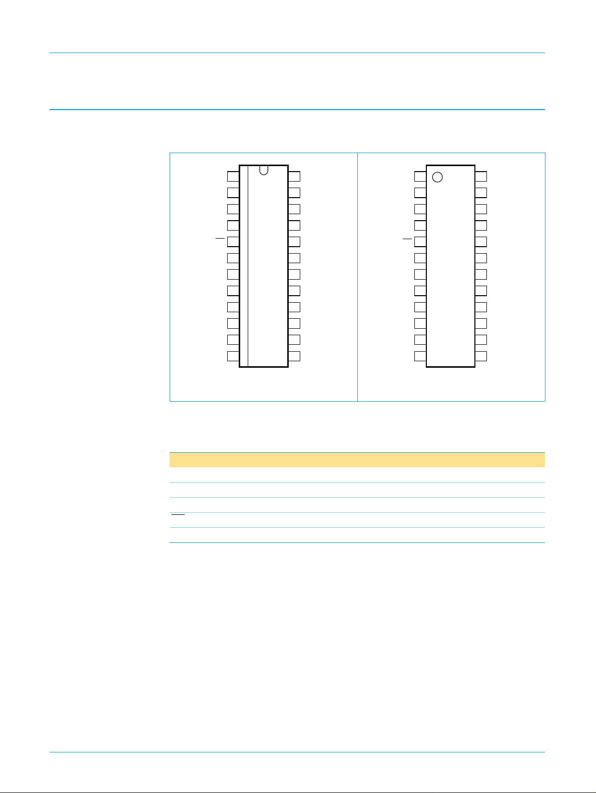
5. Pinning information
5.1 Pinning
PCK351
1:10 clock distribution device with 3-State outputs
GND
Y
V
CC
Y
OE
GND
GND
Y
V
CC
Y
GND
1
2
10
3
4
9
5
6
A
7
8
9
8
10
11
7
12
PCK351D
002aaa280
GND
24
Y
23
1
V
22
CC
Y
21
2
GND
20
Y
19
3
Y
18
4
GND
17
Y
16
5
V
15
CC
Y
14
6
GND
13
GND
Y
V
CC
Y
OE
GND
GND
Y
V
CC
Y
GND
1
2
10
3
4
9
5
6
A
7
8
9
8
10
11
7
12
002aaa281
Fig 1. SO24 pin configuration. Fig 2. SSOP24 pin configuration.
5.2 Pin description
Table 3: Pin description
Symbol Pin Description
GND 1, 7, 8, 12, 13, 17, 20, 24 ground (0 V)
to Y
Y
10
V
CC
OE 5 output enable input (Active-LOW)
A 6 data input
2, 4, 9, 11, 14, 16, 18, 19, 21, 23 outputs
1
3, 10, 15, 22 supply voltage
24
23
22
21
20
19
18
PCK351DB
17
16
15
14
13
GND
Y
1
V
CC
Y
2
GND
Y
3
Y
4
GND
Y
5
V
CC
Y
6
GND
9397 750 09791
© Koninklijke Philips Electronics N.V. 2002. All rights reserved.
Product data Rev. 01 — 14 May 2002 3 of 17
Philips Semiconductors
6. Functional description
6.1 Function table
Table 4: Function table
A OE Y
LH Z
HH Z
LL L
HL H
[1] H = HIGH voltage level;
L = LOW voltage level;
Z = high-impedance OFF-state.
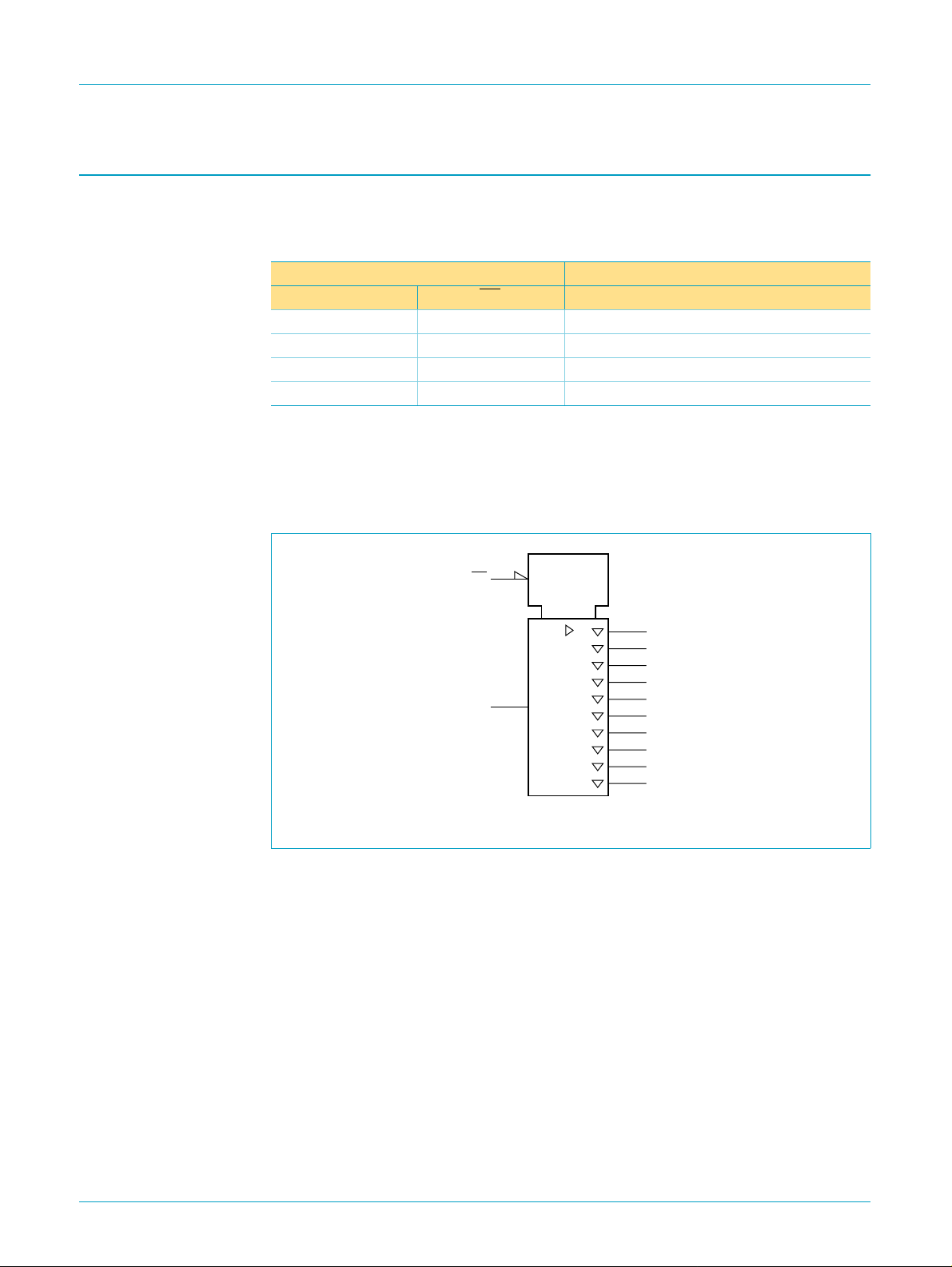
6.2 Logic symbol
PCK351
1:10 clock distribution device with 3-State outputs
Inputs Outputs
n
Fig 3. Logic symbol.
OE
5
EN
23
Y
1
21
Y
2
19
Y
3
18
Y
4
16
6
A
002aaa283
Y
5
14
Y
6
11
Y
7
9
Y
8
4
Y
9
2
Y
10
9397 750 09791
© Koninklijke Philips Electronics N.V. 2002. All rights reserved.
Product data Rev. 01 — 14 May 2002 4 of 17
Philips Semiconductors
6.3 Logic diagram
PCK351
1:10 clock distribution device with 3-State outputs
5
OE
23
Y
1
21
Y
2
19
Y
3
18
Y
6
A
4
16
Y
5
14
Y
6
11
Y
7
Fig 4. Logic diagram.
9
4
2
002aaa282
Y
8
Y
9
Y
10
9397 750 09791
© Koninklijke Philips Electronics N.V. 2002. All rights reserved.
Product data Rev. 01 — 14 May 2002 5 of 17

Philips Semiconductors
7. Limiting values
PCK351
1:10 clock distribution device with 3-State outputs
Table 5: Limiting values
In accordance with the Absolute Maximum Rating System (IEC 60134).
[1],[2]
Symbol Parameter Conditions Min Max Unit
V
CC
V
I
V
O
I
IK
I
OK
I
O
, I
I
CC
GND
T
stg
P
D
[1] Stresses beyond those listed may cause permanent damage to the device. These are stress ratings
only and functional operation of the device at these or any other conditions beyond those indicated
under ‘recommended operating conditions’ is not implied. Exposure to absolute-maximum-rated
conditions for extended periods may affect device reliability.
[2] The performance capability of a high-performance integrated circuit in conjunction with its thermal
environment can create junction temperatures which are detrimental to reliability. The maximum
junction temperature of this integrated circuit should not exceed 150 °C.
[3] The input and output negative voltage ratings may be exceeded if the input and output clamp currents
are observed.
supply voltage range −0.5 +4.6 V
input voltage range
output voltage range
[3]
−0.5 +7.0 V
[3]
−0.5 +3.6 V
input clamp current VI<0V - −18 mA
output clamp current VI<0V - −50 mA
output sink current - 64 mA
VCC or GND current - ±75 mA
storage temperature −65 +150 °C
maximum power dissipation
SO package T
SSOP package T
= +55 °C - 0.65 W
amb
= +55 °C - 1.7 W
amb
8. Recommended operating conditions
Table 6: Recommended operating conditions
See note 1.
Symbol Parameter Conditions Min Max Unit
V
CC
V
IH
V
I
T
amb
, t
t
r
f
[1] Unused pins (input or I/O) must be held HIGH or LOW.
supply voltage 3.0 3.6 V
HIGH-level input voltage 2.0 5.5 V
input voltage 0 0.8 V
ambient temperature see Table 7 “DC
input rise and fall times VCC= 3.3 ±0.3 V - 100 ns/V
−40 +85 °C
characteristics”
and Table 8 “AC
characteristics”
per device
9397 750 09791
Product data Rev. 01 — 14 May 2002 6 of 17
© Koninklijke Philips Electronics N.V. 2002. All rights reserved.

Philips Semiconductors
PCK351
1:10 clock distribution device with 3-State outputs
9. Static characteristics
Table 7: DC characteristics
Over recommended operating conditions; voltages are referenced to GND (ground = 0 V). T
Symbol Parameter Conditions Min Typ Max Unit
V
IK
V
OH
V
OL
I
LI
I
LO
I
OZ
input diode voltage VCC= 3.0 V; II= −18 mA - - −1.2 V
HIGH-level output voltage VCC= 3.0 V; IOH= −32 mA 2.0 - - V
LOW-level output voltage VCC= 3.0 V; IOL= 32 mA - - 0.5 V
input leakage current VCC= 3.6 V; VI= GND or 5.5 V - - ±1.0 µA
output leakage current VCC= 3.6 V; VO= 2.5 V −15 - −150 mA
3-State output OFF-state
VCC= 3.6 V; VO=3V
[1]
--±10 µA
current
I
CC
quiescent supply current VCC= 3.6 V; VI=VCCor GND; IO=0;
- - 0.3 mA
outputs HIGH
V
= 3.6 V; VI=VCCor GND; IO=0;
CC
- - 25 mA
outputs LOW
V
= 3.6 V; VI=VCCor GND; IO=0;
CC
- - 0.3 mA
outputs disabled
C
I
input capacitance VCC= 3.3 V; VI=VCC or GND;
-4-pF
f=10MHz
C
O
output capacitance VCC= 3.3 V; VO=VCC or GND;
-6-pF
f=10MHz
amb
=25°C.
[1] Not more than one output should be tested at a time, and the duration of the test should not exceed one second.
9397 750 09791
Product data Rev. 01 — 14 May 2002 7 of 17
© Koninklijke Philips Electronics N.V. 2002. All rights reserved.

Philips Semiconductors
PCK351
1:10 clock distribution device with 3-State outputs
10. Dynamic characteristics
Table 8: AC characteristics
GND = 0 V; tr=t
Symbol Parameter Conditions Min Typ Max Unit
= 3.3 V; T
V
CC
t
PLH/tPHL
t
PZH/tPZL
t
PHZ/tPLZ
t
sk(o)
t
sk(p)
t
sk(pr)
t
r
t
f
= 3.3 to 3.6 V; T
V
CC
t
PLH/tPHL
t
PZH/tPZL
t
PHZ/tPLZ
t
sk(o)
t
sk(p)
t
sk(pr)
t
r
t
f
≤
3.0 ns.
f
=25°C
amb
propagation delay A to Y
propagation delay OE to Y
propagation delay OE to Y
n
CL= 50 pF; see Figures 5 and 8 3.1 3.6 4.1 ns
CL= 50 pF; see Figures 6 and 8 1.8 3.8 5.5 ns
n
CL= 50 pF; see Figures 6 and 8 1.8 4.0 5.9 ns
n
output-to-output skew A to YnCL= 50 pF; see Figures 7 and 8 - 0.3 0.5 ns
pulse skew A to Y
part-to-part skew A to Y
rise time A to Y
fall time A to Y
amb
n
n
n
n
=0°C to +70 °C
propagation delay A to Y
propagation delay OE to Y
propagation delay OE to Y
n
CL= 50 pF; see Figures 7 and 8 - 0.2 0.8 ns
CL= 50 pF; see Figures 7 and 8 --1ns
CL= 50 pF; see Figures 5 and 8 ---ns
CL= 50 pF; see Figures 5 and 8 ---ns
CL= 50 pF; see Figures 5 and 8 ---ns
CL= 50 pF; see Figures 6 and 8 1.3 - 5.9 ns
n
CL= 50 pF; see Figures 6 and 8 1.7 - 6.3 ns
n
output-to-output skew A to YnCL= 50 pF; see Figures 7 and 8 - - 0.5 ns
pulse skew A to Y
n
part-to-part skew A to Y
rise time A to Y
fall time A to Y
n
n
n
CL= 50 pF; see Figures 7 and 8 - - 0.8 ns
CL= 50 pF; see Figures 7 and 8 --1ns
CL= 50 pF; see Figures 5 and 8 - - 1.5 ns
CL= 50 pF; see Figures 5 and 8 - - 1.5 ns
Table 9: Switching characteristics
Temperature and VCC coefficients over recommended operating free-air temperature and VCC range; note 1.
Symbol Parameter Conditions Max Unit
∆t
PLH(T)
temperature coefficient of LOW-to-HIGH propagation delay A to Y
note 2 65 ps/10 °C
n
(average value)
∆t
PHL(T)
temperature coefficient of HIGH-to-LOW propagation delay A to Y
note 2 45 ps/10 °C
n
(average value)
∆t
PLH(V)
VCC coefficient of LOW-to-HIGH propagation delay A to Y
n
note 3 −140 ps/100 mV
(averagevalue)
∆t
PHL(V)
VCC coefficient of HIGH-to-LOW propagation delay A to Y
n
note 3 −120 ps/100 mV
(averagevalue)
[1] These data were extracted from characterization material and are not tested at the factory.
[2] ∆t
[3] ∆t
PLH(T)
PLH(V)
and ∆t
and ∆t
are virtually independent of VCC.
PHL(T)
are virtually independent of temperature.
PHL(V)
9397 750 09791
Product data Rev. 01 — 14 May 2002 8 of 17
© Koninklijke Philips Electronics N.V. 2002. All rights reserved.

Philips Semiconductors
10.1 AC waveforms
PCK351
1:10 clock distribution device with 3-State outputs
3.0 V
A input
Yn output
0 V
V
OH
V
OL
1.5 V
0.8 V
1.5 V
t
PHL
2 V
t
r
t
PLH
t
f
002aaa289
Fig 5. The input (A) to outputs (Yn) propagation delays and rise and fall times.
3 V
OE input
output
LOW-to-OFF
OFF-to-LOW
output
HIGH-to-OFF
OFF-to-HIGH
0 V
V
CC
V
OL
V
OH
GND
1.5 V
t
PLZ
t
outputs
disabled
PHZ
VOL + 0.3 V
VOH − 0.3 V
t
PZL
1.5 V
t
PZH
1.5 V
outputs
disabled
outputs
disabled
002aaa290
Fig 6. 3-State enable and disable times.
9397 750 09791
Product data Rev. 01 — 14 May 2002 9 of 17
© Koninklijke Philips Electronics N.V. 2002. All rights reserved.

Philips Semiconductors
A input
Y1 output
t
PHL1
Y2 output
t
PHL2
Y3 output
t
PHL3
Y4 output
t
PHL4
t
PLH1
t
PLH2
t
PLH3
t
PLH4
PCK351
1:10 clock distribution device with 3-State outputs
Y5 output
t
Y6 output
Y7 output
Y8 output
Y9 output
Y10 output
t
PHL10
PHL5
t
PHL6
t
PHL7
t
PHL8
t
PHL9
t
PLH5
t
PLH6
t
PLH7
t
PLH8
t
PLH9
t
PLH10
(1) Output-to-output skew is the highest values of positive and negative edge skew:
t
sk(o)=tPLHn(max)
(2) Output pulse skew is the highest value of: t
(3) Part-to-part skew t
− t
sk(pr)
PLHn(min)
and t
sk(o)=tPHLn(max)
sk(p)
= |t
− t
PHLn(min)
PLHn
for n = 1 to 10.
− t
| for n = 1 to 10.
PHLn
represents the positive and negativeedgeskew between outputs of severaldevices operating under
identical conditions.
Fig 7. Calculation of t
sk(o)
, t
sk(p)
, and t
sk(pr)
.
002aaa286
9397 750 09791
© Koninklijke Philips Electronics N.V. 2002. All rights reserved.
Product data Rev. 01 — 14 May 2002 10 of 17

Philips Semiconductors
Fig 8. Load circuitry for switching times.
PULSE
GENERATOR
TEST S1
t
PLH/tPHL
t
PLZ/tPZL
t
PHZ/tPZH
PCK351
1:10 clock distribution device with 3-State outputs
6 V
S1
open
GND
002aaa285
V
open
6 V
GND
V
CC
I
R
T
D.U.T.
V
O
C
L
50 pF
500 Ω
500 Ω
9397 750 09791
© Koninklijke Philips Electronics N.V. 2002. All rights reserved.
Product data Rev. 01 — 14 May 2002 11 of 17

Philips Semiconductors
11. Package outline
PCK351
1:10 clock distribution device with 3-State outputs
SO24: plastic small outline package; 24 leads; body width 7.5 mm
D
c
y
Z
24
pin 1 index
1
e
13
12
w M
b
p
SOT137-1
E
H
E
Q
A
2
A
1
L
p
L
detail X
(A )
A
X
v M
A
A
3
θ
0 5 10 mm
scale
DIMENSIONS (inch dimensions are derived from the original mm dimensions)
mm
OUTLINE
VERSION
SOT137-1
A
max.
2.65
0.10
A
0.30
0.10
0.012
0.004
1
A2A3b
2.45
0.25
2.25
0.096
0.01
0.089
IEC JEDEC EIAJ
075E05 MS-013
0.49
0.36
0.019
0.014
p
0.32
0.23
0.013
0.009
UNIT
inches
Note
1. Plastic or metal protrusions of 0.15 mm maximum per side are not included.
(1)E(1) (1)
cD
15.6
15.2
0.61
0.60
REFERENCES
eHELLpQ
7.6
7.4
0.30
0.29
1.27
0.050
10.65
10.00
0.419
0.394
1.4
0.055
1.1
0.4
0.043
0.016
1.1
1.0
0.043
0.039
0.25
0.25 0.1
0.01
0.01
EUROPEAN
PROJECTION
ywv θ
Z
0.9
0.4
0.035
0.004
0.016
ISSUE DATE
97-05-22
99-12-27
o
8
o
0
Fig 9. SO24 package outline (SOT137-1).
9397 750 09791
Product data Rev. 01 — 14 May 2002 12 of 17
© Koninklijke Philips Electronics N.V. 2002. All rights reserved.

Philips Semiconductors
PCK351
1:10 clock distribution device with 3-State outputs
SSOP24: plastic shrink small outline package; 24 leads; body width 5.3 mm
D
c
y
Z
24 13
A
2
A
pin 1 index
1
SOT340-1
E
H
E
Q
L
p
L
(A )
A
X
v M
A
A
3
θ
112
b
e
DIMENSIONS (mm are the original dimensions)
UNIT A1A2A3b
Note
1. Plastic or metal protrusions of 0.20 mm maximum per side are not included.
A
max.
0.21
mm
2.0
OUTLINE
VERSION
SOT340-1 MO-150
0.05
1.80
0.25
1.65
IEC JEDEC EIAJ
p
0.38
0.25
p
cD
0.20
8.4
0.09
8.0
REFERENCES
0 2.5 5 mm
(1)E(1) (1)
Fig 10. SSOP24 package outline (SOT340-1).
detail X
w M
scale
eHELLpQZywv θ
5.4
0.65 1.25
5.2
7.9
7.6
1.03
0.63
0.9
0.7
EUROPEAN
PROJECTION
0.13 0.10.2
0.8
0.4
ISSUE DATE
95-02-04
99-12-27
o
8
o
0
9397 750 09791
© Koninklijke Philips Electronics N.V. 2002. All rights reserved.
Product data Rev. 01 — 14 May 2002 13 of 17

Philips Semiconductors
12. Soldering
12.1 Introduction to soldering surface mount packages
This text gives a very brief insight to a complex technology. A more in-depth account
of soldering ICs can be found in our
Packages
There is no soldering method that is ideal for all surface mount IC packages. Wave
soldering can still be used for certain surface mount ICs, but it is not suitable for fine
pitch SMDs. In these situations reflow soldering is recommended.
12.2 Reflow soldering
Reflow soldering requires solder paste (a suspension of fine solder particles, flux and
binding agent) to be applied to the printed-circuit board by screen printing, stencilling
or pressure-syringe dispensing before package placement.
Several methods exist for reflowing; for example, convection or convection/infrared
heating in a conveyor type oven. Throughput times (preheating, soldering and
cooling) vary between 100 and 200 seconds depending on heating method.
PCK351
1:10 clock distribution device with 3-State outputs
Data Handbook IC26; Integrated Circuit
(document order number 9398 652 90011).
Typical reflow peak temperatures range from 215 to 250 °C. The top-surface
temperature of the packages should preferable be kept below 220 °C for thick/large
packages, and below 235 °C small/thin packages.
12.3 Wave soldering
Conventional single wave soldering is not recommended for surface mount devices
(SMDs) or printed-circuit boards with a high component density, as solder bridging
and non-wetting can present major problems.
To overcome these problems the double-wave soldering method was specifically
developed.
If wave soldering is used the following conditions must be observed for optimal
results:
• Use a double-wave soldering method comprising a turbulent wave with high
upward pressure followed by a smooth laminar wave.
• For packages with leads on two sides and a pitch (e):
– larger than or equal to 1.27 mm, the footprint longitudinal axis is preferred to be
parallel to the transport direction of the printed-circuit board;
– smaller than 1.27 mm, the footprint longitudinal axis must be parallel to the
transport direction of the printed-circuit board.
The footprint must incorporate solder thieves at the downstream end.
• For packages with leads on four sides, the footprint must be placed at a 45° angle
to the transport direction of the printed-circuit board. The footprint must
incorporate solder thieves downstream and at the side corners.
9397 750 09791
Product data Rev. 01 — 14 May 2002 14 of 17
© Koninklijke Philips Electronics N.V. 2002. All rights reserved.

Philips Semiconductors
During placement and before soldering, the package must be fixed with a droplet of
adhesive. The adhesive can be applied by screen printing, pin transfer or syringe
dispensing. The package can be soldered after the adhesive is cured.
Typical dwell time is 4 seconds at 250 °C. A mildly-activated flux will eliminate the
need for removal of corrosive residues in most applications.
12.4 Manual soldering
Fix the component by first soldering two diagonally-opposite end leads. Use a low
voltage (24 V or less) soldering iron applied to the flat part of the lead. Contact time
must be limited to 10 seconds at up to 300 °C.
When using a dedicated tool, all other leads can be soldered in one operation within
2 to 5 seconds between 270 and 320 °C.
12.5 Package related soldering information
Table 10: Suitability of surface mount IC packages for wave and reflow soldering
Package
BGA, LBGA, LFBGA, SQFP, TFBGA, VFBGA not suitable suitable
HBCC, HBGA, HLQFP, HSQFP, HSOP,
HTQFP, HTSSOP, HVQFN, HVSON, SMS
PLCC
LQFP, QFP, TQFP not recommended
SSOP, TSSOP, VSO not recommended
PCK351
1:10 clock distribution device with 3-State outputs
methods
[1]
[4]
, SO, SOJ suitable suitable
Soldering method
Wave Reflow
not suitable
[3]
[4][5]
[6]
suitable
suitable
suitable
[2]
[1] For more detailed information on the BGA packages refer to the
(AN01026); order a copy from your Philips Semiconductors sales office.
[2] All surface mount (SMD) packages are moisture sensitive. Depending upon the moisture content, the
maximum temperature (with respect to time) and body size of the package, there is a risk that internal
or external package cracks may occur due to vaporization of the moisture in them (the so called
popcorn effect). For details, refer to the Drypack information in the
Circuit Packages; Section: Packing Methods
[3] These packages are not suitable for wave soldering. On versions with the heatsink on the bottom
side, the solder cannot penetratebetweentheprinted-circuitboardandtheheatsink.Onversionswith
the heatsink on the top side, the solder might be deposited on the heatsink surface.
[4] If wave soldering is considered, then the package must be placed at a 45° angle to the solder wave
direction. The package footprint must incorporate solder thieves downstream and at the side corners.
[5] Wave soldering is suitable for LQFP,QFPand TQFP packages with a pitch (e) larger than 0.8 mm; it
is definitely not suitable for packages with a pitch (e) equal to or smaller than 0.65mm.
[6] Wave soldering is suitable for SSOP and TSSOP packages with a pitch (e) equal to or larger than
0.65 mm; it is definitely not suitable for packages with a pitch (e) equal to or smaller than 0.5 mm.
.
(LF)BGA Application Note
Data Handbook IC26; Integrated
13. Revision history
Table 11: Revision history
Rev Date CPCN Description
01 20020514 - Product data; initial version. Engineering Change Notice 853-2344 28198.
9397 750 09791
Product data Rev. 01 — 14 May 2002 15 of 17
© Koninklijke Philips Electronics N.V. 2002. All rights reserved.

Philips Semiconductors
14. Data sheet status
PCK351
1:10 clock distribution device with 3-State outputs
Data sheet status
Objective data Development This data sheetcontains data from the objective specification forproduct development.Philips Semiconductors
Preliminary data Qualification This data sheet contains data from the preliminary specification. Supplementary data will be published at a
Product data Production This data sheet contains data from the product specification. Philips Semiconductors reserves the right to
[1] Please consult the most recently issued data sheet before initiating or completing a design.
[2] The product status of the device(s) described in this data sheet may have changed since this data sheet was published. The latest information is available on the Internet at
URL http://www.semiconductors.philips.com.
[1]
Product status
15. Definitions
Short-form specification — The data in a short-form specification is
extracted from a full data sheet with the same type number and title. For
detailed information see the relevant data sheet or data handbook.
Limiting values definition — Limiting values given are in accordance with
the Absolute Maximum Rating System (IEC 60134). Stress above one or
more of the limiting values may cause permanent damage to the device.
These are stress ratings only and operation of the device at these or at any
other conditions above those given in the Characteristics sections of the
specification is not implied. Exposure to limiting values for extended periods
may affect device reliability.
Application information — Applications that are described herein for any
of these products are for illustrative purposes only. Philips Semiconductors
make no representation or warranty that such applications will be suitablefor
the specified use without further testing or modification.
[2]
Definition
reserves the right to change the specification in any manner without notice.
later date. Philips Semiconductors reserves the right to change the specification without notice, in order to
improve the design and supply the best possible product.
make changes at any time in order to improve the design, manufacturing and supply. Changes will be
communicated according to the Customer Product/Process Change Notification (CPCN) procedure
SNW-SQ-650A.
16. Disclaimers
Life support — These products are not designed for use in life support
appliances, devices, or systems where malfunction of these products can
reasonably be expected to result in personal injury. Philips Semiconductors
customers using or selling these products for use in such applications do so
at their own risk and agree to fully indemnify Philips Semiconductors for any
damages resulting from such application.
Right to make changes — Philips Semiconductors reserves the right to
make changes, without notice, in the products, including circuits, standard
cells, and/or software, described or contained herein in order to improve
design and/or performance. Philips Semiconductors assumes no
responsibility or liability for the use of any of these products, conveys no
licence or title under any patent, copyright, or mask work right to these
products, and makes norepresentations or warrantiesthat these productsare
free frompatent, copyright, or maskwork right infringement, unless otherwise
specified.
Contact information
For additional information, please visit http://www.semiconductors.philips.com.
For sales office addresses, send e-mail to: sales.addresses@www.semiconductors.philips.com. Fax: +31 40 27 24825
9397 750 09791
Product data Rev. 01 — 14 May 2002 16 of 17
© Koninklijke Philips Electronics N.V. 2002. All rights reserved.

Philips Semiconductors
Contents
1 Description. . . . . . . . . . . . . . . . . . . . . . . . . . . . . 1
2 Features . . . . . . . . . . . . . . . . . . . . . . . . . . . . . . . 1
3 Quick reference data . . . . . . . . . . . . . . . . . . . . . 2
4 Ordering information. . . . . . . . . . . . . . . . . . . . . 2
5 Pinning information. . . . . . . . . . . . . . . . . . . . . . 3
5.1 Pinning . . . . . . . . . . . . . . . . . . . . . . . . . . . . . . . 3
5.2 Pin description . . . . . . . . . . . . . . . . . . . . . . . . . 3
6 Functional description . . . . . . . . . . . . . . . . . . . 4
6.1 Function table. . . . . . . . . . . . . . . . . . . . . . . . . . 4
6.2 Logic symbol. . . . . . . . . . . . . . . . . . . . . . . . . . . 4
6.3 Logic diagram. . . . . . . . . . . . . . . . . . . . . . . . . . 5
7 Limiting values. . . . . . . . . . . . . . . . . . . . . . . . . . 6
8 Recommended operating conditions. . . . . . . . 6
9 Static characteristics. . . . . . . . . . . . . . . . . . . . . 7
10 Dynamic characteristics . . . . . . . . . . . . . . . . . . 8
10.1 AC waveforms. . . . . . . . . . . . . . . . . . . . . . . . . . 9
11 Package outline . . . . . . . . . . . . . . . . . . . . . . . . 12
12 Soldering . . . . . . . . . . . . . . . . . . . . . . . . . . . . . 14
12.1 Introduction to soldering surface mount
packages . . . . . . . . . . . . . . . . . . . . . . . . . . . . 14
12.2 Reflow soldering. . . . . . . . . . . . . . . . . . . . . . . 14
12.3 Wave soldering. . . . . . . . . . . . . . . . . . . . . . . . 14
12.4 Manual soldering . . . . . . . . . . . . . . . . . . . . . . 15
12.5 Package related soldering information . . . . . . 15
13 Revision history. . . . . . . . . . . . . . . . . . . . . . . . 15
14 Data sheet status . . . . . . . . . . . . . . . . . . . . . . . 16
15 Definitions . . . . . . . . . . . . . . . . . . . . . . . . . . . . 16
16 Disclaimers. . . . . . . . . . . . . . . . . . . . . . . . . . . . 16
PCK351
1:10 clock distribution device with 3-State outputs
© Koninklijke Philips Electronics N.V. 2002.
Printed in the U.S.A
All rights are reserved. Reproduction in whole or in part is prohibited without the prior
written consent of the copyright owner.
The information presented in this document does not form part of any quotation or
contract, is believed to be accurate and reliable and may be changed without notice. No
liability will be accepted by the publisher for any consequence of its use. Publication
thereof does not convey nor imply any license under patent- or other industrial or
intellectual property rights.
Date of release: 14 May 2002 Document order number: 9397 750 09791
 Loading...