


查询PCF8831供应商查询PCF8831供应商
INTEGRATED CIRCUITS
DATA SH EET
PCF8831
STN RGB - 160 output row driver
Preliminary specification 2002 Aug 14

Philips Semiconductors Preliminary specification
STN RGB - 160 output row driver PCF8831
CONTENTS
1 FEATURES
2 APPLICATIONS
3 GENERAL DESCRIPTION
4 ORDERING INFORMATION
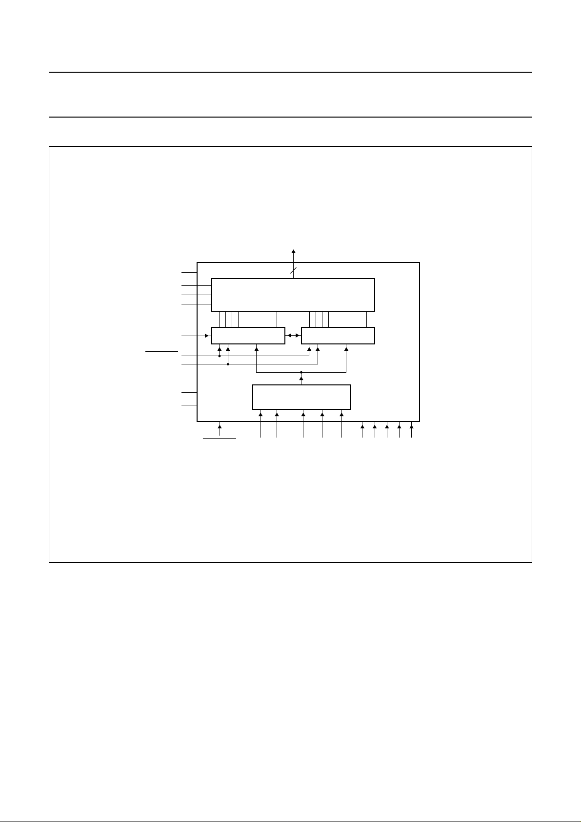
5 BLOCK DIAGRAM
6 PINNING
7 FUNCTIONAL DESCRIPTION
7.1 Row driver
7.2 80-bit shift register
7.3 Row control
7.4 Frame control
8 LIMITING VALUES
9 HANDLING
10 DC CHARACTERISTICS
11 AC CHARACTERISTICS
11.1 Power-up and power-down sequences
12 APPLICATION INFORMATION
13 INTERNAL PROTECTION CIRCUITS
14 BONDING PAD LOCATION
15 TRAY INFORMATION
16 DATA SHEET STATUS
17 DEFINITIONS
18 DISCLAIMERS
2002 Aug 14 2

Philips Semiconductors Preliminary specification
STN RGB - 160 output row driver PCF8831
1 FEATURES
• Row driver for LCD dot matrix
• 160 row outputs
• Selectable scan direction
• Support of display off function
• Support of N-line inversion
• Programmable connection to display module
• Logic supply voltage: 2.4 to 3.5 V
• Display supply voltage range: 15 to 40 V
• Low power consumption; suitable for battery operated
systems
• CMOS compatible inputs
• Manufactured in silicon gate CMOS process.
4 ORDERING INFORMATION
TYPE NUMBER
NAME DESCRIPTION VERSION
PCF8831U − chip with bumps in tray −
2 APPLICATIONS
• Mobile phones
• Personal Digital Assistant (PDA)
• Automotive information systems
• Point-of-sale terminals
• Instrumentation.
3 GENERAL DESCRIPTION
The PCF8831 is a row driver for driving colour STN
displays. It is designed to operate with the PCF8832
column driver IC.
PACKAGE
2002 Aug 14 3
Philips Semiconductors Preliminary specification
STN RGB - 160 output row driver PCF8831
5 BLOCK DIAGRAM
handbook, full pagewidth
V
MH
V
V
V
RP
ROWRES1
RCLK
V
SS
V
DD
R0 to R159
160
H
M
L
SHIFT REGISTER 1
.....
ROW DRIVERS
.....
SHIFT REGISTER 2
PCF8831
ROW CONTROL
FI
SW1SVM
T1ROWRES2 T2 T3 T4 T5SW2 R1F
MGW629
Fig.1 Block diagram.
2002 Aug 14 4

Philips Semiconductors Preliminary specification
STN RGB - 160 output row driver PCF8831
6 PINNING
SYMBOL PAD
(1)
TYPE DESCRIPTION
R159 to R0 2 to 161 O LCD row outputs
RCLK 187 I clock input to the shift register; data is transmitted with the positive clock
edge; connect RCLK to the RCLK output of the PCF8832 column driver
RP 188 I row pulse input; driven by the RP output of the PCF8832 column driver
FI 189 I frame inversion input; controls frame and N-line inversion; FI is synchronized
internally by the rising edge of RCLK; FI can change only when RP changes;
connect FI to the FI output of the PCF8832 column driver
SVM 190 I input that switches the non-selected level (V
or VSS, depending on
M
ROWRES2) to all row outputs; connect SVM to the SVM output of the
PCF8832 column driver
ROWRES1 191 I external reset input 1; when LOW, the shift register is reset at the next rising
edge of RCLK and all outputs (R0 to R159) go to their non-selected level;
connect ROWRES1 to the RESROW output of the PCF8832 column driver
ROWRES2 192 I external reset input 2; when LOW, the non-selected level goes to VSS; when
HIGH, the non-selected level goes to VM; connect ROWREST to the
RESROW output of the PCF8832 column driver
R1F 193 I inputs R1F (row block 1 first), SW1 (swap row block 1) and SW2 (swap row
SW1 194 I
SW2 195 I
block 2) control the shift direction through the register and the order of the
register; see Table 1; connect to the corresponding signal outputs of the
PCF8832 column driver, or connect directly to V
or VSS as required by the
DD
display module configuration
T1 to T5 196 to 200 I test inputs; connect to V
V
SS
V
DD
V
M
201 to 207 PS logic power supply, negative; normally connected to system ground
208 to 214 PS logic power supply, positive; 2.4 to 3.5 V referred to V
215 to 221 PS MID-level LCD driving voltage; level is between VH and VL; output at rows for
for normal operation
SS
SS
non-selecting periods when ROWRES2 is HIGH; 1.25 to 2.0 V referred to V
V
V
MH
H
222 to 228 PS auxiliary supply voltage for row switch; higher than VM; limited at VL+40V
229 to 235 PS HIGH-levelLCD driving voltage;top level of the positiveselecting pulse of row
outputs
V
L
236 to 242 PS LOW-levelLCD driving voltage; bottom levelof the negative selecting pulse of
row outputs
SS
Note
1. Dummy pads are located at positions 1 (slanted), 162 to 186 and 243 to 272.
2002 Aug 14 5
Philips Semiconductors Preliminary specification
STN RGB - 160 output row driver PCF8831
7 FUNCTIONAL DESCRIPTION
7.1 Row driver
The row driver comprises high voltage outputs, level
shifters and logic circuits.
The row driver power supplies are:
• VH for the top level of selecting pulses
• VL for the bottom level of selecting pulses
• VMforthenon-selectinglevelwhenROWRES2 = HIGH;
the non-selecting level goes to VSS when
ROWRES2 = LOW (active)
• VMH is an intermediate auxiliary supply
• VDDand VSS for the logic circuits.
dbook, full pagewidth
LCD ROW OUTPUTS
R0
.....
R79
7.2 80-bit shift register
Two shift registers of 80 bits each are contained in the
PCF8831 row driver. With ROWRES1, the complete shift
register will be reset at the next rising edge of RCLK. The
two shift registers can be configured for different
applications by row control signals R1F, SW1 and SW2.
7.3 Row control
Row control signals SW1, SW2 and R1F control the shift
direction through the register and the order of the register
(see Fig.2). Some switching combinations require the
order of one or both shift registers to be swapped as
shown by the example in Fig.3. All row control
combinations are shown in Table 1, thesecan be software
controlled when connected to the corresponding row
control signals of the PCF8832 column driver.
LCD ROW OUTPUTS
R80
.....
R159
handbook, full pagewidth
SW1
SW2
R1F
SW2 SHIFT DIRECTION
00
10
01
11
SHIFT REGISTER 1
Fig.2 Shift directions; R1F = 1.
LCD ROW OUTPUTS
R79
SW1
SW2
R1F
.....
SHIFT REGISTER 1
R0
SW1
SW2
R1F
SW1
SW2
R1F
SHIFT REGISTER 2
SHIFT DIRECTIONSW1
LCD ROW OUTPUTS
R159
SHIFT REGISTER 2
.....
MGW630
R80
MGW631
Fig.3 Row swapping; SW1 = SW2 = 1.
2002 Aug 14 6

Philips Semiconductors Preliminary specification
STN RGB - 160 output row driver PCF8831
Table 1 Row control switching
ROW CONTROL SIGNALS
R1F SW1 SW2
1 0 0 R0 to R79 R80 to R159
1 0 1 R0 to R79 R159 to R80
1 1 0 R79 to R0 R80 to R159
1 1 1 R79 to R0 R159 to R80
0 0 0 R80 to R159 R0 to R79
0 0 1 R159 to R80 R0 to R79
0 1 0 R80 to R159 R79 to R0
0 1 1 R159 to R80 R79 to R0
FIRST REGISTER
SELECTED
SECOND REGISTER
SELECTED
2002 Aug 14 7
Philips Semiconductors Preliminary specification
STN RGB - 160 output row driver PCF8831
7.4 Frame control
The signal FI controls frame inversion (Fig.4) and N-line inversion (Fig.5). Software control of FI is performed via the
PCF8832 column driver.
handbook, full pagewidth
R0
R1
R2
Frame n Frame n + 1
FI
V
H
V
M
V
L
V
H
V
M
V
L
V
H
V
M
V
L
.
.
.
.
.
.
.
.
.
.
V
H
R159
Fig.4 Frame inversion.
2002 Aug 14 8
MGW632
V
M
V
L
Philips Semiconductors Preliminary specification
STN RGB - 160 output row driver PCF8831
handbook, full pagewidth
FI
R0
R1
R2
R3
V
H
V
M
V
L
V
H
V
M
V
L
V
H
V
M
V
L
V
H
V
M
V
L
R4
R5
Fig.5 N-line inversion; N = 2.
2002 Aug 14 9
MGW633
V
H
V
M
V
L
V
H
V
M
V
L

Philips Semiconductors Preliminary specification
STN RGB - 160 output row driver PCF8831
8 LIMITING VALUES
In accordance with the Absolute Maximum Rating System (IEC 60134); note 1.
SYMBOL PARAMETER MIN. MAX. UNIT
V
DD
V
SS
V
MH
V
H
V
M
V
I
T
oper
T
stg
Note
1. Parameters are valid over the operating temperature range; all voltages are referred to V
unless otherwise specified.
logic supply positive voltage VSS− 0.3 VSS+ 7.0 V
logic supply negative voltage VL− 0.3 VL+ 40.0 V
auxiliary supply voltage for row switching VL− 0.3 VL+ 45.0 V
HIGH-level LCD driving voltage VL− 0.3 VL+45 V
MID-level LCD driving voltage VL− 0.3 VH+ 0.3 V
− 45.0 VL+ 45.0 V
V
H
V
− 0.3 VSS+ 7.0 V
SS
input voltage VSS− 0.3 VDD+ 0.3 V
operating temperature −40 +85 °C
storage temperature −65 +150 °C
substrate potential = VL;
L;
9 HANDLING
Inputs and outputs are protected against electrostatic discharge in normal handling. However, to be totally safe, it is
recommended to take normal precautions appropriate to handling MOS devices (see
“Handling MOS Devices”
).
2002 Aug 14 10

Philips Semiconductors Preliminary specification
STN RGB - 160 output row driver PCF8831
10 DC CHARACTERISTICS
(VDD− VSS) = 2.4 to 3.5 V; (VH− VL) = 15 to 55 V; T
SYMBOL PARAMETER CONDITIONS MIN. TYP. MAX. UNIT
V
L
LOW-level LCD driving
voltage
V
H
HIGH-level LCD driving
voltage
V
M
MID-level LCD driving
voltage
V
MH
auxiliary supply voltage for
row switching
V
SS
logic supply negative
voltage
V
DD
V
IH
V
IL
I
LI
R
O
I
DD
I
VH
I
VMH
I
VM
I
VL
logic supply positive voltage VSS+ 2.4 − VSS+ 3.5 V
HIGH-level input voltage all inputs; referred to V
LOW-level input voltage all inputs; referred to V
input leakage current all inputs
V
I=VDD
V
=V
I
row output on-state
resistance
current at pad V
current at pad V
current at pad V
current at pad V
current at pad V
DD
H
MH
M
L
notes 2 and 3
I
= +100 µA − 600 tbf Ω
O
I
= ±100 µA − 600 tbf Ω
O
I
= −100 µA − 600 tbf Ω
O
notes 3, 4 and 5 − 30 tbf µA
= −40 to +85 °C; unless otherwise specified.
amb
− 0 − V
VL+ 15.0 − VL+ 45.0 V
V
SS
VLVH+
--------------------
note 1 VM+10 VL+40 V
VM− 2.0 − VM− 1.25 V
SS
VSS+ 0.8 ×
− V
(VDD− VSS)
SS
V
SS
− VSS+ 0.2 ×
−−5µA
SS
−5 −−µA
− 10 tbf µA
− 3 tbf µA
− 2 tbf µA
− 13 tbf µA
V
DD
V
2
DD
V
V
(VDD− VSS)
Notes
1. The minimum level of (V
− VM) depends on (VM− VL); a lower level of (VM− VL) requires lower offset of V
MH
referred to VM. A higher level of (VMH− VM) improves dynamic behaviour. A minimum level of
(VMH− VM)=2.5V+0.2×(VM− VL) should be maintained.
2. Row outputs tested one at a time.
VHVL+
3. (V
4. f
5. Frame inversion frequency .
− VL) = 37 V; VMH=VH; (VDD− VSS) = 2.8 V; ; (VM− VSS) = 1.47 V.
H
= 19.2 kHz; SVM = 0; ROWRES1 = ROWRES2 = HIGH; single line mode; all row outputs open-circuit.
RCLK
f
f
RCLK
=
-------------------
FI
2 160×
=
V
--------------------
M
2
2002 Aug 14 11
MH

Philips Semiconductors Preliminary specification
STN RGB - 160 output row driver PCF8831
11 AC CHARACTERISTICS
(VDD− VSS) = 2.4 to 3.5 V; (VH− VL) = 15 to 55 V; T
SYMBOL PARAMETER MIN. TYP. MAX. UNIT
f
RCLK
t
RCLKL
t
RCLKH
t
r
RCLK clock frequency − 19.2 700 kHz
RCLK clock LOW time 100 −−ns
RCLK clock HIGH time 100 −−ns
input rise time RCLK, RP, FI, SVM,
ROWRES1 and ROWRES2
t
f
input fall time RCLK, RP, FI, SVM,
ROWRES1 and ROWRES2
t
su(D)
t
h(D)
data setup time RP, FI and ROWRES1 50 −−ns
data hold time RP, FI and ROWRES1 50 −−ns
= −40 to +85 °C; see Fig.6.
amb
−−50 ns
−−50 ns
handbook, full pagewidth
RCLK
RP, FI, ROWRES1
Fig.6 AC waveforms showing RCLK and data input.
t
r
t
RCLKL
t
su(D)
t
RCLKH
t
h(D)
t
f
t
f
t
r
MGW634
2002 Aug 14 12

Philips Semiconductors Preliminary specification
STN RGB - 160 output row driver PCF8831
11.1 Power-up and power-down sequences
When the PCF8831 is powering-up or powering-down, the various supply voltages and some interface signals have to
be applied in a certain sequence.
Table 2 Power-up and power-down sequences
T
= −40 to +85 °C; refer to Figs 7 and 8.
amb
SYMBOL PARAMETER CONDITIONS MIN. UNIT
t
d(VDD-VH)
t
d(VDD-VMH)
t
d(VDD-VL)
t
d(VH-VDD)
t
d(VMH-VDD)
t
d(VL-VDD)
t
PU(VH-SVM)
t
PU(VMH-SVM)
t
PU(VL-SVM)
t
rel(RES1-SVM)
t
rel(RES1)
t
rel(RES2)
t
PD(VH)
t
PD(VMH)
t
PD(VL)
delay V
delay V
delay V
delay V
delay V
delay V
power-up time V
power-up time V
power-up time V
DD(on)
DD(on)
DD(on)
H(off)
MH(off)
L(off)
to V
to V
to V
to V
to V
to V
H(on)
MH(on)
L(on)
DD(off)
DD(off)
DD(off)
to SVM inactive SVM falls to V
H(on)
to SVM inactive SVM falls to V
MH(on)
to SVM inactive SVM falls to V
L(on)
note 1 0 ns
note 1 0 ns
note 2 0 ns
note 1 0 ns
note 1 0 ns
note 2 0 ns
SS
SS
SS
ROWRES1 release time to SVM inactive release ROWRES1 before making
SVM inactive
ROWRES1 release time allow at least one rising RCLK edge
before releasing ROWRES1
ROWRES2 release time define VM when ROWRES2 is
inactive; note 3
power-down time from SVM active to V
power-down time from SVM active to V
power-down time from SVM active to V
H(off)
MH(off)
L(off)
0ns
0ns
0ns
0ns
50 ns
0ns
0ns
0ns
0ns
Notes
1. With no V
or VMH supply, both pads VHand VMH are clamped by separate internal diodes to VDD, see Fig.10.
H
2. When no VL is supplied, pad VL is clamped to VSS by a separate internal diode, see Fig.10.
3. When ROWRES2 is active (at VSS), the level not-selected goes to VSS and pad VM can be disconnected.
2002 Aug 14 13

Philips Semiconductors Preliminary specification
STN RGB - 160 output row driver PCF8831
handbook, full pagewidth
ROWRES1
V
DD
V
H
V
MH
V
L
SVM
t
d(VDD-VH)
t
d(VDD-VMH)
(1)
t
d(VDD-VL)
(2)
t
rel(RES1-SVM)
V
DD
V
SS
V
(1)
t
PU(VH-SVM)
t
PU(VMH-SVM)
t
PU(VL-SVM)
H
> VSS + 8 V
V
MH
> VSS + 8 V
< VSS − 5.5 V
V
L
RCLK
t
rel(RES1)
V
M
ROWRES2
(1) With no VHor VMH supply, both pads VHand VMH are clamped by separate internal diodes to VDD; see Table 2 and Fig.10.
(2) When no VLis supplied, pad VLis clamped to VSS by a separate internal diode; see Table 2 and Fig.10.
(3) When ROWRES2 is active (at VSS), the level not-selected goes to VSS and VM can be disconnected; see Table 2 and Fig.10.
(3)
t
rel(RES2)
MGW635
Fig.7 Power-up sequence.
2002 Aug 14 14
V
M

Philips Semiconductors Preliminary specification
STN RGB - 160 output row driver PCF8831
handbook, full pagewidth
V
DD
V
H
V
MH
V
L
SVM
V
M
t
PD(VH)
t
PD(VMH)
t
PD(VL)
t
rel(RES2)
t
d(VH-VDD)
(1)
t
d(VMH-VDD)
(1)
t
d(VL-VDD)
V
DD
V
SS
(2)
(3)
ROWRES2
(1) With no VHor VMH supply, both pads VHand VMH are clamped by separate internal diodes to VDD; see Table 2 and Fig.10.
(2) When no VLis supplied, pad VLis clamped to VSS by a separate internal diode; see Table 2 and Fig.10.
(3) When ROWRES2 is active (at VSS), the level not-selected goes to VSS and pad VM can be disconnected; see Table 2 and Fig.10.
MGW636
Fig.8 Power-down sequence.
2002 Aug 14 15

Philips Semiconductors Preliminary specification
STN RGB - 160 output row driver PCF8831
12 APPLICATION INFORMATION
handbook, full pagewidth
V
DD
V
COL
LCK
R2
R1
T1 to T5
V
V
MH
V
(1)
H
L
V
V
DD
PCF8831
M
V
SS
(2)
9
R0
R159
Row control
V
160
V
COL
LCK
FBQ
M
C0
V
DD1VDD3
V
DD2
LCD DISPLAY
(128 × 160 dots)
384
PCF8832
V
SS
C383
CA2CA1
MGW637
(1) Test inputs T1 to T5 have to be tied to VSS.
(2) Row control signals are RCLK, RP, FI, SVM, RESROW1, RESROW2, SW1, SW2 and R1F.
Fig.9 Application example using PCF8831 with PCF8832.
2002 Aug 14 16

Philips Semiconductors Preliminary specification
STN RGB - 160 output row driver PCF8831
13 INTERNAL PROTECTION CIRCUITS
handbook, full pagewidth
V
H
pads 229 to 235
V
MH
pads 222 to 228
V
M
pads 215 to 221
V
L
pads 236 to 242
RCLK
RP
FI
SVM
ROWRES1
ROWRES2
R1F
SW1
SW2
T1
T2
T3
T4
T5
pad 187
188
189
190
191
192
193
194
195
196
197
198
199
200
V
H
V
MH
V
DD
pads 208 to 214
V
SS
pads 201 to 207
V
DD
V
SS
V
H
R0 to R159
pads 161 to 2
V
L
V
DD
V
M
V
SS
V
L
MGW639
Protection diode maximum forward current = 5 mA.
Fig.10 Protection circuit diagrams.
2002 Aug 14 17

Philips Semiconductors Preliminary specification
STN RGB - 160 output row driver PCF8831
14 BONDING PAD INFORMATION
Table 3 Pad locations
All x and y coordinates are referenced to the centre of the
chip (dimensions in µm; see Fig.13)
SYMBOL PAD x y
Dummy
(slanted)
R159 2 −5984.0 −768.0
R158 3 −5909.0 −768.0
R157 4 −5834.0 −768.0
R156 5 −5759.0 −768.0
R155 6 −5684.0 −768.0
R154 7 −5609.0 −768.0
R153 8 −5534.0 −768.0
R152 9 −5459.0 −768.0
R151 10 −5384.0 −768.0
R150 11 −5309.0 −768.0
R149 12 −5234.0 −768.0
R148 13 −5159.0 −768.0
R147 14 −5084.0 −768.0
R146 15 −5009.0 −768.0
R145 16 −4934.0 −768.0
R144 17 −4859.0 −768.0
R143 18 −4784.0 −768.0
R142 19 −4709.0 −768.0
R141 20 −4634.0 −768.0
R140 21 −4559.0 −768.0
R139 22 −4484.0 −768.0
R138 23 −4409.0 −768.0
R137 24 −4334.0 −768.0
R136 25 −4259.0 −768.0
R135 26 −4184.0 −768.0
R134 27 −4109.0 −768.0
R133 28 −4034.0 −768.0
R132 29 −3959.0 −768.0
R131 30 −3884.0 −768.0
R130 31 −3809.0 −768.0
R129 32 −3734.0 −768.0
R128 33 −3659.0 −768.0
R127 34 −3584.0 −768.0
R126 35 −3509.0 −768.0
R125 36 −3434.0 −768.0
1 −6116.0 −768.0
SYMBOL PAD x y
R124 37 −3359.0 −768.0
R123 38 −3284.0 −768.0
R122 39 −3209.0 −768.0
R121 40 −3134.0 −768.0
R120 41 −3059.0 −768.0
R119 42 −2984.0 −768.0
R118 43 −2909.0 −768.0
R117 44 −2834.0 −768.0
R116 45 −2759.0 −768.0
R115 46 −2684.0 −768.0
R114 47 −2609.0 −768.0
R113 48 −2534.0 −768.0
R112 49 −2459.0 −768.0
R111 50 −2384.0 −768.0
R110 51 −2309.0 −768.0
R109 52 −2234.0 −768.0
R108 53 −2159.0 −768.0
R107 54 −2084.0 −768.0
R106 55 −2009.0 −768.0
R105 56 −1934.0 −768.0
R104 57 −1859.0 −768.0
R103 58 −1784.0 −768.0
R102 59 −1709.0 −768.0
R101 60 −1634.0 −768.0
R100 61 −1559.0 −768.0
R99 62 −1484.0 −768.0
R98 63 −1409.0 −768.0
R97 64 −1334.0 −768.0
R96 65 −1259.0 −768.0
R95 66 −1184.0 −768.0
R94 67 −1109.0 −768.0
R93 68 −1034.0 −768.0
R92 69 −959.0 −768.0
R91 70 −884.0 −768.0
R90 71 −809.0 −768.0
R89 72 −734.0 −768.0
R88 73 −659.0 −768.0
R87 74 −584.0 −768.0
R86 75 −509.0 −768.0
R85 76 −434.0 −768.0
R84 77 −359.0 −768.0
2002 Aug 14 18

Philips Semiconductors Preliminary specification
STN RGB - 160 output row driver PCF8831
SYMBOL PAD x y
R83 78 −284.0 −768.0
R82 79 −209.0 −768.0
R81 80 −134.0 −768.0
R80 81 −59.0 −768.0
R79 82 +91.0 −768.0
R78 83 +166.0 −768.0
R77 84 +241.0 −768.0
R76 85 +316.0 −768.0
R75 86 +391.0 −768.0
R74 87 +466.0 −768.0
R73 88 +541.0 −768.0
R72 89 +616.0 −768.0
R71 90 +691.0 −768.0
R70 91 +766.0 −768.0
R69 92 +841.0 −768.0
R68 93 +916.0 −768.0
R67 94 +991.0 −768.0
R66 95 +1066.0 −768.0
R65 96 +1141.0 −768.0
R64 97 +1216.0 −768.0
R63 98 +1291.0 −768.0
R62 99 +1366.0 −768.0
R61 100 +1441.0 −768.0
R60 101 +1516.0 −768.0
R59 102 +1591.0 −768.0
R58 103 +1666.0 −768.0
R57 104 +1741.0 −768.0
R56 105 +1816.0 −768.0
R55 106 +1891.0 −768.0
R54 107 +1966.0 −768.0
R53 108 +2041.0 −768.0
R52 109 +2116.0 −768.0
R51 110 +2191.0 −768.0
R50 111 +2266.0 −768.0
R49 112 +2341.0 −768.0
R48 113 +2416.0 −768.0
R47 114 +2491.0 −768.0
R46 115 +2566.0 −768.0
R45 116 +2641.0 −768.0
R44 117 +2716.0 −768.0
R43 118 +2791.0 −768.0
SYMBOL PAD x y
R42 119 +2866.0 −768.0
R41 120 +2941.0 −768.0
R40 121 +3016.0 −768.0
R39 122 +3091.0 −768.0
R38 123 +3166.0 −768.0
R37 124 +3241.0 −768.0
R36 125 +3316.0 −768.0
R35 126 +3391.0 −768.0
R34 127 +3466.0 −768.0
R33 128 +3541.0 −768.0
R32 129 +3616.0 −768.0
R31 130 +3691.0 −768.0
R30 131 +3766.0 −768.0
R29 132 +3841.0 −768.0
R28 133 +3916.0 −768.0
R27 134 +3991.0 −768.0
R26 135 +4066.0 −768.0
R25 136 +4141.0 −768.0
R24 137 +4216.0 −768.0
R23 138 +4291.0 −768.0
R22 139 +4366.0 −768.0
R21 140 +4441.0 −768.0
R20 141 +4516.0 −768.0
R19 142 +4591.0 −768.0
R18 143 +4666.0 −768.0
R17 144 +4741.0 −768.0
R16 145 +4816.0 −768.0
R15 146 +4891.0 −768.0
R14 147 +4966.0 −768.0
R13 148 +5041.0 −768.0
R12 149 +5116.0 −768.0
R11 150 +5191.0 −768.0
R10 151 +5266.0 −768.0
R9 152 +5341.0 −768.0
R8 153 +5416.0 −768.0
R7 154 +5491.0 −768.0
R6 155 +5566.0 −768.0
R5 156 +5641.0 −768.0
R4 157 +5716.0 −768.0
R3 158 +5791.0 −768.0
R2 159 +5866.0 −768.0
2002 Aug 14 19

Philips Semiconductors Preliminary specification
STN RGB - 160 output row driver PCF8831
SYMBOL PAD x y
R1 160 +5941.0 −768.0
R0 161 +6016.0 −768.0
Dummy 162 +6155.0 −768.0
Dummy 163 6096.5 865.7
Dummy 164 6021.5 865.7
Dummy 165 5796.5 865.7
Dummy 166 5721.5 865.7
Dummy 167 5646.5 865.7
Dummy 168 5571.5 865.7
Dummy 169 5496.5 865.7
Dummy 170 5421.5 865.7
Dummy 171 5346.5 865.7
Dummy 172 5271.5 865.7
Dummy 173 5196.5 865.7
Dummy 174 5121.5 865.7
Dummy 175 5046.5 865.7
Dummy 176 4971.5 865.7
Dummy 177 4896.5 865.7
Dummy 178 4821.5 865.7
Dummy 179 4746.5 865.7
Dummy 180 4671.5 865.7
Dummy 181 4596.5 865.7
Dummy 182 4521.5 865.7
Dummy 183 4446.5 865.7
Dummy 184 3921.5 865.7
Dummy 185 3846.5 865.7
Dummy 186 3771.5 865.7
RCLK 187 3506.0 865.7
RP 188 3350.0 865.7
FI 189 3186.0 865.7
SVM 190 3030.0 865.7
ROWRES1 191 2866.0 865.7
ROWRES2 192 2710.0 865.7
R1F 193 2546.0 865.7
SW1 194 2214.0 865.7
SW2 195 2050.0 865.7
T1 196 1894.0 865.7
T2 197 1730.0 865.7
T3 198 1574.0 865.7
T4 199 1410.0 865.7
T5 200 1254.0 865.7
SYMBOL PAD x y
V
SS
V
SS
V
SS
V
SS
V
SS
V
SS
V
SS
V
DD
V
DD
V
DD
V
DD
V
DD
V
DD
V
DD
V
M
V
M
V
M
V
M
V
M
V
M
V
M
V
MH
V
MH
V
MH
V
MH
V
MH
V
MH
V
MH
V
H
V
H
V
H
V
H
V
H
V
H
V
H
V
L
V
L
V
L
V
L
V
L
V
L
201 1139.0 865.7
202 1064.0 865.7
203 989.0 865.7
204 865.0 865.7
205 790.0 865.7
206 661.5 865.7
207 586.5 865.7
208 326.7 865.7
209 251.7 865.7
210 176.7 865.7
211 101.7 865.7
212 26.7 865.7
213 −48.3 +865.7
214 −123.3 +865.7
215 −882.9 +865.7
216 −957.9 +865.7
217 −1032.9 +865.7
218 −1107.9 +865.7
219 −1182.9 +865.7
220 −1257.9 +865.7
221 −1332.9 +865.7
222 −1630.7 +865.7
223 −1705.7 +865.7
224 −1780.7 +865.7
225 −1855.7 +865.7
226 −1930.7 +865.7
227 −2005.7 +865.7
228 −2080.7 +865.7
229 −2334.3 +865.7
230 −2409.3 +865.7
231 −2484.3 +865.7
232 −2559.3 +865.7
233 −2634.3 +865.7
234 −2709.3 +865.7
235 −2784.3 +865.7
236 −3013.5 +865.7
237 −3088.5 +865.7
238 −3163.5 +865.7
239 −3238.5 +865.7
240 −3313.5 +865.7
241 −3388.5 +865.7
2002 Aug 14 20

Philips Semiconductors Preliminary specification
STN RGB - 160 output row driver PCF8831
SYMBOL PAD x y
V
L
242 −3463.5 +865.7
Dummy 243 −3728.5 +865.7
Dummy 244 −3803.5 +865.7
Dummy 245 −3878.5 +865.7
Dummy 246 −3953.5 +865.7
Dummy 247 −4103.5 +865.7
Dummy 248 −4178.5 +865.7
Dummy 249 −4253.5 +865.7
Dummy 250 −4328.5 +865.7
Dummy 251 −4403.5 +865.7
Dummy 252 −4478.5 +865.7
Dummy 253 −4553.5 +865.7
Dummy 254 −4628.5 +865.7
Dummy 255 −4703.5 +865.7
Dummy 256 −4778.5 +865.7
Dummy 257 −4853.5 +865.7
Dummy 258 −4928.5 +865.7
Dummy 259 −5003.5 +865.7
Dummy 260 −5078.5 +865.7
Dummy 261 −5153.5 +865.7
Dummy 262 −5228.5 +865.7
SYMBOL PAD x y
Dummy 263 −5303.5 +865.7
Dummy 264 −5378.5 +865.7
Dummy 265 −5453.5 +865.7
Dummy 266 −5528.5 +865.7
Dummy 267 −5603.5 +865.7
Dummy 268 −5678.5 +865.7
Dummy 269 −5753.5 +865.7
Dummy 270 −5978.5 +865.7
Dummy 271 −6053.5 +865.7
Dummy 272 −6128.5 +865.7
Alignment marks (see Fig.12)
Alignment circle 1 5909.0 865.7
Alignment circle 2 −5866.0 +865.7
Table 4 Bonding pad dimensions
PAD SIZE UNIT
Minimum pad pitch 75 µm
Pad size; aluminium tbf µm
Bump dimensions 50 × 80 × 17.5 (±5) µm
Wafer thickness
381 µm
(excluding bumps)
handbook, halfpage
2.36
mm
12.66 mm
PCF8831
pitch
MGW640
Fig.11 Bonding pads.
2002 Aug 14 21
handbook, halfpage
y centre
100
µm
x centre
MGS688
Fig.12 Alignment mark detail.

Philips Semiconductors Preliminary specification
STN RGB - 160 output row driver PCF8831
handbook, full pagewidth
pad 163
circle 2
pad 186
RCLK
SVM
ROWRES1
ROWRES2
R1F
SW1
SW2
V
SS
V
DD
RP
pad 162
R0
.
.
.
.
.
PC8831-1
FI
T1
T2
T3
T4
T5
.
.
x
0,0
y
.
.
.
R79
R80
.
.
.
.
.
12.66
mm
Dummy bump
Alignment mark
Circles 1 and 2 are alignment marks (see Fig.12).
V
M
V
MH
V
H
V
L
pad 243
circle 1
pad 272
2.238 mm
Fig.13 Bonding pad location.
.
.
.
.
.
R159
pad 1
MGW638
2002 Aug 14 22

Philips Semiconductors Preliminary specification
STN RGB - 160 output row driver PCF8831
15 TRAY INFORMATION
handbook, full pagewidth
The dimensions are given in Table 5.
x
y
F
A
E
C
D
B
MGS488
Fig.14 Tray details.
handbook, halfpage
PCF8831
MGW641
The orientationof the IC in a pocketis indicated by the position ofthe
IC type name on the die surface with respect to the chamfer on the
upper left corner of the tray. Refer to the bonding pad location
diagram for the orientation and position of the type name on the die
surface.
Fig.15 Tray alignment.
2002 Aug 14 23
Table 5 Tray dimensions
DIMENSIONS DESCRIPTION VALUE
A pocket pitch, x direction 14.86 mm
B pocket pitch, y direction 4.45 mm
C pocket width, x direction 12.76 mm
D pocket width, y direction 2.34 mm
E tray width, x direction 50.8 mm
F tray width, y direction 50.8 mm
− number of pockets in
3
x direction
− number of pockets in
10
y direction

Philips Semiconductors Preliminary specification
STN RGB - 160 output row driver PCF8831
16 DATA SHEET STATUS
PRODUCT
DATA SHEET STATUS
Objective data Development This data sheet contains data from the objective specification for product
Preliminary data Qualification This data sheet contains data from the preliminary specification.
Product data Production This data sheet contains data from the product specification. Philips
Notes
1. Please consult the most recently issued data sheet before initiating or completing a design.
2. The product status of the device(s) described in this data sheet may have changed since this data sheet was
published. The latest information is available on the Internet at URL http://www.semiconductors.philips.com.
(1)
STATUS
(2)
development. Philips Semiconductors reserves the right to change the
specification in any manner without notice.
Supplementary data will be published at a later date. Philips
Semiconductors reserves the right to change the specification without
notice, in order to improve the design and supply the best possible
product.
Semiconductors reserves the right to make changes at any time in order
to improve the design, manufacturing and supply. Changes will be
communicated according to the Customer Product/Process Change
Notification (CPCN) procedure SNW-SQ-650A.
DEFINITIONS
17 DEFINITIONS
Short-form specification The data in a short-form
specification is extracted from a full data sheet with the
same type number and title. For detailed information see
the relevant data sheet or data handbook.
Limiting values definition Limiting values given are in
accordance with the Absolute Maximum Rating System
(IEC 60134). Stress above one or more of the limiting
values may cause permanent damage to the device.
These are stress ratings only and operation of the device
atthese or at anyotherconditionsabove those given inthe
Characteristics sections of the specification is not implied.
Exposure to limiting values for extended periods may
affect device reliability.
Application information Applications that are
described herein for any of these products are for
illustrative purposes only. Philips Semiconductors make
norepresentationorwarranty that such applications willbe
suitable for the specified use without further testing or
modification.
18 DISCLAIMERS
Life support applications These products are not
designed for use in life support appliances, devices, or
systems where malfunction of these products can
reasonably be expected to result inpersonal injury. Philips
Semiconductorscustomersusingor selling these products
for use in such applications do so at their own risk and
agree to fully indemnify Philips Semiconductors for any
damages resulting from such application.
Right to make changes Philips Semiconductors
reserves the right to make changes, without notice, in the
products, including circuits, standard cells, and/or
software, described or contained herein in order to
improve design and/or performance. Philips
Semiconductors assumes no responsibility or liability for
theuseof any of these products,conveysnolicence or title
under any patent, copyright, or mask work right to these
products,and makes no representationsorwarranties that
these products are free from patent, copyright, or mask
work right infringement, unless otherwise specified.
Bare die All die are tested and are guaranteed to
comply with all data sheet limits up to the point of wafer
sawing for a period of ninety (90) days from the date of
Philips' delivery. If there are data sheet limits not
guaranteed, these will be separately indicated in the data
sheet. There are no post packing tests performed on
individual die or wafer. Philips Semiconductors has no
control of third party procedures in the sawing, handling,
packing or assembly of the die. Accordingly, Philips
Semiconductors assumes no liability for device
functionality or performance of the die or systems after
third party sawing, handling, packing or assembly of the
die. It is the responsibility of the customer to test and
qualify their application in which the die is used.
2002 Aug 14 24

Philips Semiconductors Preliminary specification
STN RGB - 160 output row driver PCF8831
NOTES
2002 Aug 14 25

Philips Semiconductors Preliminary specification
STN RGB - 160 output row driver PCF8831
NOTES
2002 Aug 14 26

Philips Semiconductors Preliminary specification
STN RGB - 160 output row driver PCF8831
NOTES
2002 Aug 14 27

Philips Semiconductors – a w orldwide compan y
Contact information
For additional information please visit http://www.semiconductors.philips.com. Fax: +31 40 27 24825
For sales offices addresses send e-mail to: sales.addresses@www.semiconductors.philips.com.
© Koninklijke Philips Electronics N.V. 2002
All rights are reserved. Reproduction in whole or in part is prohibited without the prior written consent of the copyright owner.
The information presented in this document does not form part of any quotation or contract, is believed to be accurate and reliable and may be changed
without notice. No liability will be accepted by the publisher for any consequence of its use. Publication thereof does not convey nor imply any license
under patent- or other industrial or intellectual property rights.
Printed in The Netherlands 403512/01/pp28 Date of release: 2002 Aug 14 Document order number: 9397 750 09145
SCA74
 Loading...