

Page 1

查询PCA5097供应商
INTEGRATED CIRCUITS
DATA SH EET
PCD5090; PCA5097
DECT baseband controllers
Objective specification
File under Integrated Circuits, IC17
1996 Oct 17
Page 2

Philips Semiconductors Objective specification
DECT baseband controllers PCD5090; PCA5097
INTRODUCTION
This data sheet details the specific features of the:
PCD5090/xxx; DSP-ROM, with external ROM
PCA5097/xxx; DSP-ROM, with Field Electronically
Erasable Programmable Read Only Memory
(FEEPROM).
• On-chip reference voltage
FEATURES
General
• The PCx509x is designed for GAP-compliant handsets
and simple base stations
• Embedded 80C51 microcontroller with twice the
performance of the classic architecture, up to
128 kbytes external memory or 64 kbytes FEEPROM
program memory and 3 kbytes of data memory on chip.
In addition there is 1 kbyte of on-chip data memory that
is shared with on-chip Burst Mode Logic (BML) and
DSP, the System Data RAM (SDR).
• 80C51 ports P0, P1, P2 and P3 available for interfacing
to display, keyboard, I
external memory. External program memory is
addressable up to 128 kbytes (PCD5090/xxx and
PCA5097/xxx).
• Portable Part (PP) and Fixed Part (FP) modes
• TDMA frame (de)multiplexing; transmission or reception
can be programmed for any slot
• Ciphering, scrambling, CRC checking/generation,
protected B-fields
• Speech and data buffering space for six handsets
• Local call and B-field loop-back
• Two interrupt lines for BML and DSP to interrupt 80C51
• On-chip, three-channel time-multiplexed 8-bit
Analog-to-Digital Converter (ADC) for RSSI
measurement and battery voltage measurement. One
channel available for other purposes.
• On-chip 8-bit DAC for frequency adjustment of
13.824 MHz on-chip crystal oscillator
• Phase error measurement and phase error correction by
hardware
• Digital-to-Analog Converters (DACs) and ADCs for
dynamic earpiece and dynamic or electret microphone
2
C-bus, interrupt sources and/or
• On-chip supply for electret microphone
• Very low ohmic buzzer output
• Serial interface to external ADPCM CODEC (PCD5032)
• IOM-2interface (Siemens registered trademark)
• Serial interface to synthesizer for frequency
programming
• Programmable timing of radio-control signals
• Programmable polarity of radio-control signals
• Easy interfacing with radio circuits, operating at other
supply voltage
• Programmable GMSK pulse shaper
• On-chip comparator for use as bit-slicer
• Power-on reset
• Low supply voltage (2.7 to 5.5 V)
• SACMOS technology.
DSP software features
• ADPCM encoding and decoding complying with G.721
• Speech filters
• Programmable gain in speech paths
• Side tone and soft mute
• Ringer and tone (DTMF) generator
• Dial tone detection
• Echo cancellation
• Automatic gain control
• Telephone Answering Machine (TAM) switch
• Conference call (PCD5090/400)
• Hands-free operation (PCD5090/311).
For each DSP software version a separate manual is
available, in which detailed information is provided on how
parameters must be set.
1996 Oct 17 2
Page 3

Philips Semiconductors Objective specification
DECT baseband controllers PCD5090; PCA5097
ORDERING INFORMATION
TYPE
NUMBER
PCD5090H
PCA5097H
PCD5090HZ LQFP100 plastic low profile quad flat package; 100 leads; body 14 × 14 × 1.4 mm SOT407-1
NAME DESCRIPTION VERSION
QFP100
plastic quad flat package; 100 leads (lead length 1.95 mm); body
14 × 20 × 2.8 mm
PACKAGE
SOT317-2
1996 Oct 17 3
Page 4
Philips Semiconductors Objective specification
DECT baseband controllers PCD5090; PCA5097
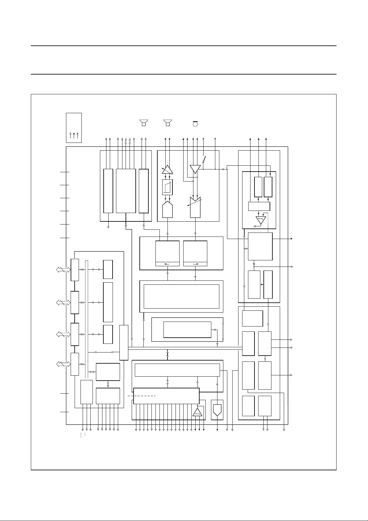
BLOCK DIAGRAM
digital pins
analog pins
supply pins
TST1
TST2
CLK3
DCK
BZP
BZM
EARP
DI
DO
FS1
EARM
LIFP
LIFM
MICP
MICM
VMIC
ref
V
VANLI
RSSI_AN
VBAT
DDA
V
SSA
V
DD
2 ×
V
SS
2 ×
V
DD_RF
V
SS_RF
V
PORT 3.7
PORT 3.0 to
PORT 2.7
PORT 2.0 to
8 8 8
PORT 1.7
PORT 1.0 to
8
PORT 0.7
PORT 0.0 to
DD_FEE
V
SS_FEE
V
DD
V
PORT 3
PORT 1 PORT 2
PORT 0
IB-BUS
80CL51- CORE
(TCB)
TEST CONTROL BLOCK
DD
V
C-BUS
2
I
(256 BYTES)
MICROCONTROLLER_RAM
AUX-RAM
(3 kBYTES)
FEEPROM
(64 kBYTES)
PGMFEE
(SPI)
IOM/ADPCM
SPEECH INTERFACE
(ABB)
BUZZER BUFFER
DD
V
MICROCONTROLLER
DD
V
DD
V
INTERFACE (ABCIF)
AB-MICROCONTROLLER
DD
V
DD_RF
V
MGE610
VANLO
handbook, full pagewidth
Fig.1 Functional blocks and signals in PCx509x.
EN_WATCHDOG RESET_OUT M_RESET VBGP
PEAK-HOLD
3 : 1
MUX
ANALOG
SOURCE
VOLTAGE
(AVR)
REFERENCE
OF
(DCA)
ANALOG
RESET
WATCHDOG
XTAL
ref
V
SUBTRACT
ADC
V
(AVS)
(POR)
POWER-ON RESET
(RGE)
GENERATOR
(WDT)
TIMER
(XOSC)
OSCILLATOR
CDC-on
ARA
ARF
ARD
1-BIT ADC
DDA
V
s
108f
(DNS)
NOISE
DIGITAL
SHAPER
s
4f
SIGNAL
DIGITAL
(BML)
MODE
LOGIC
BURST
LEVEL
SHIFTER
Σ ∆
s
108f
DIGITAL
DECIMATING
s
4f
(DSP)
PROCESSOR
RAM
DATA
(SDR)
SYSTEM
AMP
ATS
1-BIT ADC
(DDF)
FILTER
(1 kBYTE)
V
DDA
CODEC
AGM
AUXILIARY ADC (AAD)
DDA
V
DIGITAL
CONTROL
ISB BUS
CONTROLLER
BLOCK
TIMING CONTROL
CLOCK
GENERATOR
DD
V
ref
V
ANALOG VOLTAGE
(IBC)
(TICB)
(CLG)
PSE
EA
ALE
PGM
WEN
SC
SDI
OEN
SDO/A16
R_PWR
SLICE_CTR
REF_CLK
R_ENABLE
SYNTH_LOCK
S_CLK
S_DATA
S_ENABLE
S_PWR
ANT_SW1
ANT_SW0
VCO_BND_SW
1996 Oct 17 4
T_DATA
T_ENABLE
T_PWR_RMP
R_DATAP
R_DATAM
R_SLICED
T_GMSK
GP_CLK7
DPLL_DATA
XTAL1
XTAL2
CLK100
Page 5

Philips Semiconductors Objective specification
DECT baseband controllers PCD5090; PCA5097
PIN TYPE PIN DESCRIPTION
STATE
AFTER
RESET
I/O
PIN
QFP100 LQFP100
ADPCM output or IOM data clock input/output
(ISF2UPES in PCD5090/xxx, PCA5097/xxx)
ISF2UPES
15 13 −−supply negative supply voltage for RF interface level shifters
16 14 −−supply positive supply voltage for RF interface level shifters
17 15 −−supply positive supply voltage for FEEPROM program memory
SYMBOL
ANT_SW1 1 99 O H ISP2DRF3 antenna switch 1 output
ANT_SW0 2 100 O H ISP2DRF3 antenna switch 0 output
CLK100 3 1 O H ISP2DPES 100 Hz signal related to DECT frame timing output
T_ENABLE 4 2 O H ISP2DRF3 enable transmitter output
T_PWR_RMP 5 3 O L ISP2DRF3 switch transmitter power output
T_DATA 6 4 O off ISF2DRF3 unmodulated transmitter data output
T_GMSK 7 5 O L ANAIOD1 GMSK modulated transmitter data output
VCO_BND_SW 8 6 O L ISP2DRF3 VCO band switch output
SYNTH_LOCK 9 7 I − DIPP0RF3 synthesizer lock input
S_ENABLE 10 8 O L ISP2DRF3 synthesizer enable output
S_DATA 11 9 O L ISP2DRF3 serial synthesizer data output
PINNING
S_CLK 12 10 O L ISP2DRF3 clock for serial synthesizer interface output
1996 Oct 17 5
SS_RF
DD_RF
S_PWR 13 11 O H ISP2DRF3 switch synthesizer power output
REF_CLK 14 12 O running ISP4DRF3 13.824 MHz reference clock for synthesizer output
V
DD_FEE
V
V
SLICE_CTR 18 16 O L ISP2DRF3 switch slicer time constant output
R_PWR 19 17 O H ISP2DRF3 switch receiver power output
R_DATAP 20 18 I − ANAIOD2 positive input for receiver data
R_DATAM 21 19 I − ANAIOD2 negative input for receiver data
R_ENABLE 22 20 O H ISP2DRF3 enable receiver output
RSSI_AN 23 21 I − ANAIOD1 analog input for RSSI measurement
VANLI 24 22 I − ANAIOD1 analog input to A/D converter
VBAT 25 23 I − ANAIOD1 analog input for battery voltage measurement
CLK3 26 24 O L ISP2DPES 3.456 MHz clock output for external ADPCM codec
DCK 27 25 I/O input ISF2DPES
DI 28 26 I − DIPP0PES ADPCM or IOM data input
Page 6

Philips Semiconductors Objective specification
DECT baseband controllers PCD5090; PCA5097
8 kHz framing input/output
(ISF2UPES in PCD5090/xxx, PCA5097/xxx)
PIN TYPE PIN DESCRIPTION
STATE
AFTER
ISF2UPES
RESET
I/O
PIN
QFP100 LQFP100
38 36 −−supply negative supply voltage for analog circuits
42 40 O 2.0 V ANAIOD1 reference voltage (+2 V)
44 42 −−supply positive supply voltage for analog circuits
PCA5090 and PCD5090/xxx
SYMBOL
FS1 29 27 I/O input ISF2DPES
DO 30 28 O off ISI8DPES ADPCM or IOM data output
XTAL2 31 29 O running ANAIOD1 crystal oscillator output
XTAL1 32 30 I − ANAIOD1 crystal oscillator input
VANLO 33 31 O 1.0 V ANAIOD1 analog output from D/A converter
TST2 34 32 I − DIDP0PES test input 2
TST1 35 33 I − DIDP0PES test input 1
LIFM 36 34 I 0.7 V ANAIOD1 negative input from line interface
SSA
LIFP 37 35 I 0.7 V ANAIOD1 positive input from line interface
V
MICM 39 37 I 0.7 V ANAIOR1 negative input from microphone
MICP 40 38 I 0.7 V ANAIOR1 positive input from microphone
VMIC 41 39 O off ANAIOD1 positive microphone supply voltage (+2 V)
1996 Oct 17 6
ref
V
DDA
VBGP 43 41 O 1.25 V ANAIOR1 bandgap output voltage (+1.25 V)
V
EARM 45 43 O 1.4 V ANAIOD1 negative output to earpiece
EARP 46 44 O 1.4 V ANAIOD1 positive output to earpiece
EN_WATCHDOG 47 45 I − DIUP0PES watchdog enable input
P1.0 48 46 I/O H ISQ2CPES bidirectional 80C51 port pin
P1.1 49 47 I/O H ISQ2CPES bidirectional 80C51 port pin
P1.2 50 48 I/O H ISQ2CPES bidirectional 80C51 port pin
GP_CLK7 51 49 O L ISP2DPES general purpose 6.912 MHz output
DPLL_DATA 52 50 O L ISP2DPES data after clock recovery network
R_SLICED 53 51 O L ISP2DPES R_DATA comparator output
PGM 54 52 I − DIDP0PES FEEPROM programming mode; can be left open-circuit for
P1.3 55 53 I/O H ISQ2CPES bidirectional 80C51 port pin
P1.4 56 54 I/O H ISQ2CPES bidirectional 80C51 port pin
P1.5 57 55 I/O H ISQ2CPES bidirectional 80C51 port pin
Page 7

Philips Semiconductors Objective specification
DECT baseband controllers PCD5090; PCA5097
PIN TYPE PIN DESCRIPTION
STATE
AFTER
RESET
I/O
PIN
QFP100 LQFP100
60 58 −−supply positive supply voltage
63 61 −−supply negative supply voltage
64 62 −−supply negative supply voltage
for PCA5090, PCD5090/xxx
DD
can be left open-circuit for PCA5090, PCD5090/xxx
can be left open-circuit for PCA5090, PCD5090/xxx
PCD5090/xxx, PCA5097/xxx: FEEPROM shift data out/address
bit 16 for 128 kbytes external program memory
tie to V
can be left open-circuit for PCA5090, PCD5090/xxx
ISP4DPES PCA5090,PCA5097: FEEPROM shift data output
L
SYMBOL
P1.6 58 56 I/O off ISI8DPES bidirectional 80C51 port pin
DD2
P1.7 59 57 I/O off ISI8DPES bidirectional 80C51 port pin
V
BZM 61 59 O L ANAIOD2 negative buzzer output
SS2
V
SS_FEE
V
P3.0 65 63 I/O H ISQ2CPES bidirectional 80C51 port pin
P3.1 66 64 I/O H ISQ2CPES bidirectional 80C51 port pin
P3.2 67 65 I/O H ISQ2CPES bidirectional 80C51 port pin
BZP 62 60 O L ANAIOD2 positive buzzer output
P3.3 68 66 I/O H ISQ2CPES bidirectional 80C51 port pin
P3.4 69 67 I/O H ISQ2CPES bidirectional 80C51 port pin
P3.5 70 68 I/O H ISQ2CPES bidirectional 80C51 port pin
1996 Oct 17 7
P3.6 71 69 I/O H ISQ2CPES bidirectional 80C51 port pin
P3.7 72 70 I/O H ISQ2CPES bidirectional 80C51 port pin
P2.0 73 71 I/O H ISQ2CPES bidirectional 80C51 port pin
P2.1 74 72 I/O H ISQ2CPES bidirectional 80C51 port pin
P2.2 75 73 I/O H ISQ2CPES bidirectional 80C51 port pin
SDO/A16 76 74 O H or L
SC 78 76 I − DIDP0PES FEEPROM shift clock;
SDI 79 77 I − DIDP0PES FEEPROM shift data input;
OEN 77 75 I − DIDP0PES FEEPROM output enable;
WEN 80 78 I − DIUP0PES FEEPROM Write enable;
P2.3 81 79 I/O H ISQ2CPES bidirectional 80C51 port pin
P2.4 82 80 I/O H ISQ2CPES bidirectional 80C51 port pin
Page 8

Philips Semiconductors Objective specification
DECT baseband controllers PCD5090; PCA5097
PIN TYPE PIN DESCRIPTION
STATE
AFTER
RESET
I/O
PIN
QFP100 LQFP100
bidirectional 80C51 port pin
(ISQ2CPES in PCD5090/xxx, PCA5097/xxx)
bidirectional 80C51 port pin
(ISQ2CPES in PCD5090/xxx, PCA5097/xxx)
bidirectional 80C51 port pin
ISP2DPES
ISQ2CPES
ISP2DPES
ISQ2CPES
ISP2DPES
H
H
89 87 −−supply negative supply voltage
90 88 −−supply positive supply voltage
(ISQ2CPES in PCD5090/xxx, PCA5097/xxx)
bidirectional 80C51 port pin
(ISQ2CPES in PCD5090/xxx, PCA5097/xxx)
bidirectional 80C51 port pin
(ISQ2CPES in PCD5090/xxx, PCA5097/xxx)
bidirectional 80C51 port pin
(ISQ2CPES in PCD5090/xxx, PCA5097/xxx)
bidirectional 80C51 port pin
(ISQ2CPES in PCD5090/xxx, PCA5097/xxx)
bidirectional 80C51 port pin
(ISQ2CPES in PCD5090/xxx, PCA5097/xxx)
ISQ2CPES
ISP2DPES
ISQ2CPES
ISP2DPES
ISQ2CPES
ISP2DPES
ISQ2CPES
ISP2DPES
ISQ2CPES
ISP2DPES
ISQ2CPES
H
H
H
H
H
H
SYMBOL
SS1
P2.5 83 81 I/O H ISQ2CPES bidirectional 80C51 port pin
P2.6 84 82 I/O H ISQ2CPES bidirectional 80C51 port pin
P2.7 85 83 I/O H ISQ2CPES bidirectional 80C51 port pin
PSE 86 84 O H ISQ2CPES program store enable (80C51)
ALE 87 85 O H ISQ4CPES address latch enable (80C51)
EA 88 86 I − ISF2DPES external access enable (80C51)
DD1
V
V
P0.7 91 89 I/O off
P0.6 92 90 I/O off
P0.5 93 91 I/O off
1996 Oct 17 8
P0.4 94 92 I/O off
P0.3 95 93 I/O off
P0.2 96 94 I/O off
P0.1 97 95 I/O off
P0.0 98 96 I/O off
M_RESET 99 97 I − DIDP0PES master reset input (Schmitt-trigger)
RESET_OUT 100 98 O H ISF2DPES reset output
Page 9

Philips Semiconductors Objective specification
DECT baseband controllers PCD5090; PCA5097
handbook, full pagewidth
T_ENABLE
T_PWR_RMP
VCO_BND_SW
SYNTH_LOCK
S_ENABLE
SLICE_CTR
R_ENABLE
ANT_SW1
ANT_SW0
CLK100
T_DATA
T_GMSK
S_DATA
S_CLK
S_PWR
REF_CLK
V
SS_RF
V
DD_RF
V
DD_FEE
R_PWR
R_DATAP
R_DATAM
RSSI_AN
VANLI
VBAT
CLK3
DCK
FS1
DO
RESET_OUT
M_RESET
P0.0
P0.1
P0.2
P0.3
P0.4
P0.5
99989796959493929190898887868584838281
100
1
2
3
4
5
6
7
8
9
10
11
12
13
14
15
16
17
18
19
20
21
22
23
24
25
26
27
DI
28
29
30
P0.6
P0.7
V
PCA5097
PCD5090
DD1VSS1
EA
ALE
PSE
P2.7
P2.6
P2.5
P2.4
P2.3
80
WEN
79
SDI
78
SC
OEN
77
SDO/A16
76
75
P2.2
P2.1
74
P2.0
73
P3.7
72
71
P3.6
P3.5
70
P3.4
69
P3.3
68
67
P3.2
P3.1
66
P3.0
65
V
64
V
63
BZP
62
BZM
61
V
60
59
P1.7
P1.6
58
P1.5
57
P1.4
56
55
P1.3
PGM
54
R_SLICED
53
DPLL_DATA
52
GP_CLK7
51
SS_FEE
SS2
DD2
31323334353637383940414243444546474849
SSA
LIFP
LIFM
TST2
XTAL2
XTAL1
VANLO
TST1
MICM
V
Fig.2 Pin configuration of PCX509x (QFP100).
1996 Oct 17 9
MICP
VMIC
50
MGE575
ref
V
DDA
V
VBGP
EARM
P1.0
EARP
EN_WATCHDOG
P1.1
P1.2
Page 10

Philips Semiconductors Objective specification
DECT baseband controllers PCD5090; PCA5097
handbook, full pagewidth
CLK100
T_ENABLE
T_PWR_RMP
T_DATA
T_GMSK
VCO_BND_SW
SYNTH_LOCK
S_ENABLE
S_DATA
S_CLK
S_PWR
REF_CLK
V
SS_RF
V
DD_RF
V
DD_FEE
SLICE_CTR
R_PWR
R_DATAP
R_DATAM
R_ENABLE
RSSI_AN
VANLI
VBAT
CLK3
DCK
RESET_OUT
M_RESET
P0.0
P0.1
P0.2
P0.3
P0.4
ANT_SW1
ANT_SW0
99989796959493929190898887868584838281
100
1
2
3
4
5
6
7
8
9
10
11
12
13
14
15
16
17
18
19
20
21
22
23
24
P0.5
P0.6
P0.7
PCD5090
DD1VSS1
V
EA
ALE
PSE
P2.7
P2.6
P2.5
WEN
P2.4
P2.3
SDI
8079787776
SC
75
74
73
72
71
70
69
68
67
66
65
64
63
62
61
60
59
58
57
56
55
54
53
52
5125
OEN
SDO/A16
P2.2
P2.1
P2.0
P3.7
P3.6
P3.5
P3.4
P3.3
P3.2
P3.1
P3.0
V
SS_FEE
V
SS2
BZP
BZM
V
DD2
P1.7
P1.6
P1.5
P1.4
P1.3
PGM
R_SLICED
26272829303132333435363738394041424344454647484950
DI
DO
FS1
XTAL2
XTAL1
TST2
VANLO
TST1
LIFM
LIFP
SSA
V
Fig.3 Pin configuration of PCD5090/xxx only (LQFP100).
1996 Oct 17 10
MICM
MICP
VMIC
MGD744
ref
V
DDA
V
VBGP
EARM
P1.0
EARP
EN_WATCHDOG
P1.1
P1.2
GP_CLK7
DPLL_DATA
Page 11

Philips Semiconductors Objective specification
DECT baseband controllers PCD5090; PCA5097
FUNCTIONAL DESCRIPTION
DECT controller system description
The PCX509x is a family of single-chip controllers,
designed for use in Digital Enhanced Cordless
Telecommunications (DECT) systems. The family is
designed for minimal component-count and minimum
power consumption. All controllers include an embedded
80C51 microcontroller with on-chip memory and I
The Philips DECT RF-Interface is implemented. The Burst
Mode Logic performs the time-critical MAC layer functions
for applications in DECT handsets and base stations.
The ADPCM transcoding is in compliance with the CCITT
recommendation G.721 and includes receive and transmit
filters.
Power-on reset logic and power management functions
further reduce power consumption and external
components. The chip is intended to support stand-alone
systems only. There are no provisions to build clusters of
base stations. There are no provisions for external
controllers to exert control over the embedded 80C51 or to
have direct access to the on-chip data memories.
The DECT controller consists of a number of functional
blocks that operate more or less autonomously and
communicate with each other via the System Data RAM
(SDR). Blocks have access to SDR via the Internal System
Bus (ISB). The ISB consists of an 8-bit data, a 10-bit
address bus and a number of bus-request/bus-grant
signals. Access to the ISB is controlled by ISB bus
Controller (IBC). The IBC acknowledges bus requests on
the basis of a priority scheme.
2
C-bus.
A-fields and B-fields are stored in separate buffers. In this
way, two traffic bearers, each with their private A-fields,
can share the same B-field buffer as is required in case of
bearer hand-over or local call.
The blocks DSP and CODEC support speech processing
functions such as A/D- and D/A conversion, filtering,
ADPCM encoding and decoding, 8-bit A-law PCM to 14-bit
linear PCM conversion and its reverse, echo cancelling,
tone generation, etc.
PCA5097
This chip is intended for program development. It contains
64 kbytes of internal program memory (FEEPROM) for the
80C51 and DSP program RAM.
PCD5090/xxx
This chip is intended for handset and base station
applications. The DSP program is now fixed in a ROM, for
which several ROM codes (/xxx) are available (handset,
analog base, digital base). An external program memory
for the 80C51 of 128 kbytes ROM can be handled.
PCA5097/xxx
This is the same as PCD5090/xxx, but there is 64 kbytes
internal program memory (FEEPROM) for the 80C51.
The DSP program is preprogrammed in ROM.
This chip is meant for development purpose only.
The embedded controller 80C51 is to be programmed by
the user. It must contain DECT software from
Man-Machine-Interface (MMI) to the DECT protocols TBC,
CBC and DBC (refer to figures 10, 11, 12 and 13 in
“prETS 300 175-2:1992 section 6”
All software is available from Philips Semiconductors.
Hardware state machines in the Burst Mode Logic (BML)
and the Speech Interface (SPI) execute the lower blocks in
the TBC, CBC and DBC. The 80C51 has control over the
BML and the SPI via tables in SDR. The BML saves serial
data, received via R_DATAP/M, in buffer areas in SDR.
The position of buffers in SDR is fixed by the 80C51
software by means of tables previously mentioned.
1996 Oct 17 11
).
Page 12

Philips Semiconductors Objective specification
DECT baseband controllers PCD5090; PCA5097
handbook, full pagewidth
handbook, full pagewidth
EARPIECE
RADIO
CIRCUITS
PCx509x
MICROPHONE
MGE586
a. Handset.
RADIO
CIRCUITS
PCx509x
LINE
INTERFACE
(e.g. PCD1070)
a/b line
MGD745
b. Base with analog interface and echo cancellation; up to 6 portables can be handled.
handbook, full pagewidth
RADIO
CIRCUITS
c. Base with digital interface and analog handset connected; up to 6 portables can be handled.
Fig.4 Block diagrams of DECT systems with PCx509x.
1996 Oct 17 12
PCx509x
MICROPHONE
2 x IOM or
2
2 x ADPCM-CODEC or
a combination
EARPIECE
MGD746
Page 13

Philips Semiconductors Objective specification
DECT baseband controllers PCD5090; PCA5097
PACKAGE OUTLINES
QFP100: plastic quad flat package; 100 leads (lead length 1.95 mm); body 14 x 20 x 2.8 mm
c
y
X
E
e
w M
p
A
A
H
E
E
2
A
A
1
80 51
81
pin 1 index
100
1
50
Z
b
31
30
detail X
SOT317-2
Q
L
p
L
(A )
3
θ
w M
b
e
p
Z
D
D
H
D
0 5 10 mm
scale
DIMENSIONS (mm are the original dimensions)
mm
A
max.
3.20
0.25
0.05
2.90
2.65
0.25
UNIT A1A2A3b
cE
p
0.40
0.25
0.25
0.14
(1)
(1) (1)(1)
D
20.1
19.9
eH
14.1
13.9
0.65
24.2
23.6
Note
1. Plastic or metal protrusions of 0.25 mm maximum per side are not included.
OUTLINE
VERSION
IEC JEDEC EIAJ
REFERENCES
SOT317-2
1996 Oct 17 13
v M
A
B
v M
B
H
D
LLpQZywv θ
E
18.2
17.6
1.0
0.6
1.4
1.2
0.15 0.10.21.95
EUROPEAN
PROJECTION
Z
D
0.8
1.0
0.4
0.6
ISSUE DATE
E
o
7
o
0
92-11-17
95-02-04
Page 14

Philips Semiconductors Objective specification
DECT baseband controllers PCD5090; PCA5097
LQFP100: plastic low profile quad flat package; 100 leads; body 14 x 14 x 1.4 mm
c
y
100
X
75
76
51
50
Z
E
pin 1 index
26
1
e
w M
b
p
25
Z
D
D
H
D
b
B
e
w M
p
v M
v M
A
H
E
E
A
2
A
A
1
A
B
detail X
SOT407-1
Q
(A )
3
θ
L
p
L
0 5 10 mm
scale
DIMENSIONS (mm are the original dimensions)
UNIT
mm
A
A1A2A3bpcE
max.
0.20
1.6
0.05
1.5
1.3
0.25
0.28
0.16
0.18
0.12
(1)
(1) (1)(1)
D
14.1
13.9
eH
H
14.1
13.9
0.5
16.25
15.75
Note
1. Plastic or metal protrusions of 0.25 mm maximum per side are not included.
OUTLINE
VERSION
IEC JEDEC EIAJ
REFERENCES
SOT407-1
1996 Oct 17 14
D
LLpQZywv θ
E
16.25
15.75
0.75
0.45
0.70
0.57
0.12 0.10.21.0
EUROPEAN
PROJECTION
Z
D
1.15
1.15
0.85
0.85
ISSUE DATE
E
o
7
o
0
95-12-19
Page 15

Philips Semiconductors Objective specification
DECT baseband controllers PCD5090; PCA5097
SOLDERING
Introduction
There is no soldering method that is ideal for all IC
packages. Wave soldering is often preferred when
through-hole and surface mounted components are mixed
on one printed-circuit board. However, wave soldering is
not always suitable for surface mounted ICs, or for
printed-circuits with high population densities. In these
situations reflow soldering is often used.
This text gives a very brief insight to a complex technology.
A more in-depth account of soldering ICs can be found in
our
“IC Package Databook”
Reflow soldering
Reflow soldering techniques are suitable for all LQFP and
QFP packages.
The choice of heating method may be influenced by larger
plastic QFP packages (44 leads, or more). If infrared or
vapour phase heating is used and the large packages are
not absolutely dry (less than 0.1% moisture content by
weight), vaporization of the small amount of moisture in
them can cause cracking of the plastic body. For more
information, refer to the Drypack chapter in our
Reference Handbook”
Reflow soldering requires solder paste (a suspension of
fine solder particles, flux and binding agent) to be applied
to the printed-circuit board by screen printing, stencilling or
pressure-syringe dispensing before package placement.
Several techniques exist for reflowing; for example,
thermal conduction by heated belt. Dwell times vary
between 50 and 300 seconds depending on heating
method. Typical reflow temperatures range from
215 to 250 °C.
(order code 9398 652 90011).
“Quality
(order code 9397 750 00192).
Wave soldering
Wave soldering is not recommended for LQFP or QFP
packages. This is because of the likelihood of solder
bridging due to closely-spaced leads and the possibility of
incomplete solder penetration in multi-lead devices.
If wave soldering cannot be avoided, the following
conditions must be observed:
• A double-wave (a turbulent wave with high upward
pressure followed by a smooth laminar wave)
soldering technique should be used.
• The footprint must be at an angle of 45° to the board
direction and must incorporate solder thieves
downstream and at the side corners.
Even with these conditions:
• Do not consider wave soldering LQFP packages
LQFP48 (SOT313-2), LQFP64 (SOT314-2) or
LQFP80 (SOT315-1).
• Do not consider wave soldering QFP packages
QFP52 (SOT379-1), QFP100 (SOT317-1),
QFP100 (SOT317-2), QFP100 (SOT382-1) or
QFP160 (SOT322-1).
During placement and before soldering, the package must
be fixed with a droplet of adhesive. The adhesive can be
applied by screen printing, pin transfer or syringe
dispensing. The package can be soldered after the
adhesive is cured.
Maximum permissible solder temperature is 260 °C, and
maximum duration of package immersion in solder is
10 seconds, if cooled to less than 150 °C within
6 seconds. Typical dwell time is 4 seconds at 250 °C.
A mildly-activated flux will eliminate the need for removal
of corrosive residues in most applications.
Preheating is necessary to dry the paste and evaporate
the binding agent. Preheating duration: 45 minutes at
45 °C.
1996 Oct 17 15
Repairing soldered joints
Fix the component by first soldering two diagonallyopposite end leads. Use only a low voltage soldering iron
(less than 24 V) applied to the flat part of the lead. Contact
time must be limited to 10 seconds at up to 300 °C. When
using a dedicated tool, all other leads can be soldered in
one operation within 2 to 5 seconds between
270 and 320 °C.
Page 16

Philips Semiconductors Objective specification
DECT baseband controllers PCD5090; PCA5097
DEFINITIONS
Data sheet status
Objective specification This data sheet contains target or goal specifications for product development.
Preliminary specification This data sheet contains preliminary data; supplementary data may be published later.
Product specification This data sheet contains final product specifications.
Short-form specification The data in this specification is extracted from a full data sheet with the same type
number and title. For detailed information see the relevant data sheet or data handbook.
Limiting values
Limiting values given are in accordance with the Absolute Maximum Rating System (IEC 134). Stress above one or
more of the limiting values may cause permanent damage to the device. These are stress ratings only and operation
of the device at these or at any other conditions above those given in the Characteristics sections of the specification
is not implied. Exposure to limiting values for extended periods may affect device reliability.
Application information
Where application information is given, it is advisory and does not form part of the specification.
LIFE SUPPORT APPLICATIONS
These products are not designed for use in life support appliances, devices, or systems where malfunction of these
products can reasonably be expected to result in personal injury. Philips customers using or selling these products for
use in such applications do so at their own risk and agree to fully indemnify Philips for any damages resulting from such
improper use or sale.
2
PURCHASE OF PHILIPS I
C COMPONENTS
2
Purchase of Philips I
components in the I2C system provided the system conforms to the I2C specification defined by
Philips. This specification can be ordered using the code 9398 393 40011.
C components conveys a license under the Philips’ I2C patent to use the
1996 Oct 17 16
 Loading...