


DATA SH EET
Product specification
Supersedes data of 1997 Oct 21
File under Integrated Circuits, IC18
2000 Jan 13
INTEGRATED CIRCUITS
PCA82C250
CAN controller interface
2000 Jan 13 2
Philips Semiconductors Product specification
CAN controller interface PCA82C250
FEATURES
• Fully compatible with the
“ISO 11898”
standard
• High speed (up to 1 Mbaud)
• Bus lines protected against transients in an automotive
environment
• Slope control to reduce Radio Frequency Interference
(RFI)
• Differential receiver with wide common-mode range for
high immunity against ElectroMagnetic Interference
(EMI)
• Thermally protected
• Short-circuit proof to battery and ground
• Low-current standby mode
• An unpowered node does not disturb the bus lines
• At least 110 nodes can be connected.
APPLICATIONS
• High-speed applications (up to 1 Mbaud) in cars.
GENERAL DESCRIPTION
The PCA82C250 is the interface between the CAN
protocol controller and the physical bus. The device
provides differential transmit capability to the bus and
differential receive capability to the CAN controller.
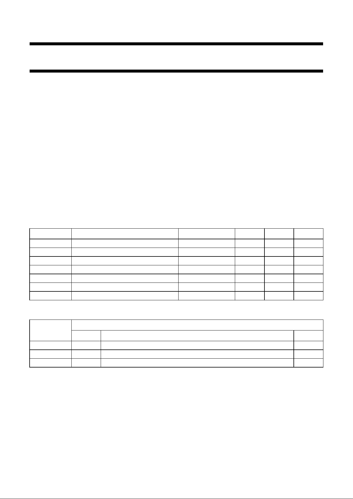
QUICK REFERENCE DATA
ORDERING INFORMATION
SYMBOL PARAMETER CONDITIONS MIN. MAX. UNIT
V
CC
supply voltage 4.5 5.5 V
I
CC
supply current standby mode − 170 µA
1/t
bit
maximum transmission speed non-return-to-zero 1 − Mbaud
V
CAN
CANH, CANL input/output voltage −8 +18 V
V
diff
differential bus voltage 1.5 3.0 V
t
PD
propagation delay high-speed mode − 50 ns
T
amb
ambient temperature −40 +125 °C
TYPE
NUMBER
PACKAGE
NAME DESCRIPTION CODE
PCA82C250 DIP8 plastic dual in-line package; 8 leads (300 mil) SOT97-1
PCA82C250T SO8 plastic small outline package; 8 leads; body width 3.9 mm SOT96-1
PCA82C250U − bare die; 2790 × 1780 × 380 µm −

2000 Jan 13 3
Philips Semiconductors Product specification
CAN controller interface PCA82C250
BLOCK DIAGRAM
handbook, full pagewidth
MKA669
RECEIVER
HS
REFERENCE
VOLTAGE
SLOPE/
STANDBY
PROTECTION
DRIVER
3
2
5
4
8
1
6
7
GND
CANL
CANH
V
ref
TXD
Rs
RXD
V
CC
PCA82C250
Fig.1 Block diagram.
PINNING
SYMBOL PIN DESCRIPTION
TXD 1 transmit data input
GND 2 ground
V
CC
3 supply voltage
RXD 4 receive data output
V
ref
5 reference voltage output
CANL 6 LOW-level CAN voltage
input/output
CANH 7 HIGH-level CAN voltage
input/output
Rs 8 slope resistor input
handbook, halfpage
1
2
3
4
8
7
6
5
MKA670
PCA82C250
Rs
CANHGND
CANL
V
ref
RXD
V
CC
TXD
Fig.2 Pin configuration.

2000 Jan 13 4
Philips Semiconductors Product specification
CAN controller interface PCA82C250
FUNCTIONAL DESCRIPTION
The PCA82C250 is the interface between the CAN
protocol controller and the physical bus. It is primarily
intended for high-speed applications (up to 1 Mbaud) in
cars. Thedevice provides differential transmit capability to
the bus and differential receive capability to the CAN
controller. It is fully compatible with the
“ISO 11898”
standard.
A current limiting circuit protects the transmitter output
stage againstshort-circuit to positive and negative battery
voltage. Although the power dissipation is increased
during this fault condition, this feature will prevent
destruction of the transmitter output stage.
If the junction temperature exceeds a value of
approximately 160 °C, the limiting current of both
transmitter outputs is decreased. Because the transmitter
is responsible for the major part of the power dissipation,
this will result in a reduced powerdissipation and hence a
lowerchip temperature.All otherparts of theIC willremain
in operation.The thermal protection is particularly needed
when a bus line is short-circuited.
The CANH and CANL lines are also protected against
electrical transients which may occur in an automotive
environment.
Pin 8 (Rs) allows three different modes of operation to be
selected: high-speed, slope control or standby.
For high-speed operation, the transmitter output
transistors are simply switched on and off as fast as
possible. In this mode, no measures are taken to limit the
rise and fall slope. Use of a shielded cable is
recommended to avoid RFI problems. The high-speed
mode is selected by connecting pin 8 to ground.
For lower speeds or shorter bus length, an unshielded
twisted pair or a parallel pair of wires can be used for the
bus. To reduce RFI, the rise and fall slope should be
limited. The rise and fall slope can be programmed with a
resistor connected from pin 8 to ground. The slope is
proportional to the current output at pin 8.
If a HIGH level is applied to pin 8, the circuit enters a low
current standby mode. In this mode, the transmitter is
switched off and the receiver is switched to a low current.
If dominant bits are detected (differential bus voltage
>0.9 V), RXD will be switched to a LOW level.
The microcontroller should react to this condition by
switching the transceiver back to normal operation (via
pin 8). Because the receiver is slow in standby mode, the
first message will be lost.
Table 1 Truth table of the CAN transceiver
Note
1. X = don’t care.
Table 2 Pin Rs summary
SUPPLY TXD CANH CANL BUS STATE RXD
4.5 to 5.5 V 0 HIGH LOW dominant 0
4.5 to 5.5 V 1 (or floating) floating floating recessive 1
<2 V (not powered) X
(1)
floating floating recessive X
(1)
2V<VCC< 4.5 V >0.75V
CC
floating floating recessive X
(1)
2V<VCC< 4.5 V X
(1)
floating if
VRs> 0.75V
CC
floating if
VRs> 0.75V
CC
recessive X
(1)
CONDITION FORCED AT PIN Rs MODE RESULTING VOLTAGE OR CURRENT AT PIN Rs
V
Rs
> 0.75V
CC
standby IRs< 10 µA
−10 µA<I
Rs
< −200 µA slope control 0.4VCC<VRs< 0.6V
CC
VRs< 0.3V
CC
high-speed IRs< −500 µA
2000 Jan 13 5
Philips Semiconductors Product specification
CAN controller interface PCA82C250
LIMITING VALUES
In accordance with the Absolute Maximum Rating System (IEC 60134); all voltages are referenced to pin 2;
positive input current.
Notes
1. In accordance with
“IEC 60747-1”
. An alternative definition of virtual junction temperature is:
Tvj=T
amb+Pd×Rth(vj-a)
, where R
th(j-a)
is a fixed value to be used for the calculation of Tvj. The rating for Tvj limits
the allowable combinations of power dissipation (Pd) and ambient temperature (T
amb
).
2. Classification A: human body model; C = 100 pF; R = 1500 Ω; V = ±2000 V.
3. Classification B: machine model; C = 200 pF; R = 25 Ω; V = ±200 V.
THERMAL CHARACTERISTICS
QUALITY SPECIFICATION
According to
“SNW-FQ-611 part E”
.
SYMBOL PARAMETER CONDITIONS MIN. MAX. UNIT
V
CC
supply voltage −0.3 +9.0 V
V
n
DC voltage at pins 1, 4, 5 and 8 −0.3 VCC+ 0.3 V
V
6, 7
DC voltage at pins 6 and 7 0 V < VCC< 5.5 V;
no time limit
−8.0 +18.0 V
V
trt
transient voltage at pins 6 and 7 see Fig.8 −150 +100 V
T
stg
storage temperature −55 +150 °C
T
amb
ambient temperature −40 +125 °C
T
vj
virtual junction temperature note 1 −40 +150 °C
V
esd
electrostatic discharge voltage note 2 −2000 +2000 V
note 3 −200 +200 V
SYMBOL PARAMETER CONDITIONS VALUE UNIT
R
th(j-a)
thermal resistance from junction to ambient in free air
PCA82C250 100 K/W
PCA82C250T 160 K/W
2000 Jan 13 6
Philips Semiconductors Product specification
CAN controller interface PCA82C250
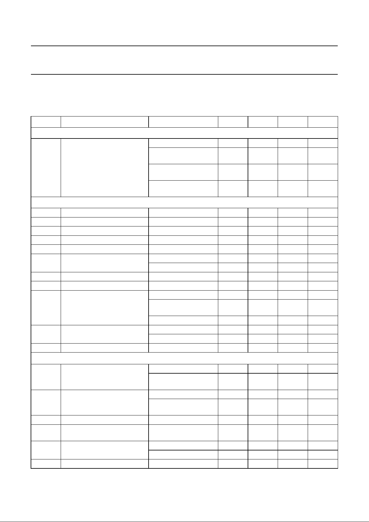
CHARACTERISTICS
VCC= 4.5 to 5.5 V; T
amb
= −40 to +125 °C; RL=60Ω; I8> −10 µA; unless otherwise specified; all voltages referenced
to ground (pin 2); positive input current; all parameters are guaranteed over the ambient temperature range by design,
but only 100% tested at +25 °C.
SYMBOL PARAMETER CONDITIONS MIN. TYP. MAX. UNIT
Supply
I
3
supply current dominant; V1=1V −−70 mA
recessive; V
1
=4V;
R8=47kΩ
−−14 mA
recessive; V
1
=4V;
V8=1V
−−18 mA
standby; T
amb
<90°C;
note 1
− 100 170 µA
DC bus transmitter
V
IH
HIGH-level input voltage output recessive 0.7V
CC
− VCC+ 0.3 V
V
IL
LOW-level input voltage output dominant −0.3 − 0.3V
CC
V
I
IH
HIGH-level input current V1=4V −200 − +30 µA
I
IL
LOW-level input current V1=1V −100 −−600 µA
V
6,7
recessive bus voltage V1= 4 V; no load 2.0 − 3.0 V
I
LO
off-state output leakage current −2V<(V6,V7)<7V −2 − +1 mA
−5V<(V
6,V7
)<18V −5 − +12 mA
V
7
CANH output voltage V1= 1 V 2.75 − 4.5 V
V
6
CANL output voltage V1= 1 V 0.5 − 2.25 V
∆V
6, 7
difference between output
voltage at pins 6 and 7
V1= 1 V 1.5 − 3.0 V
V
1
=1V; RL=45Ω;
VCC≥ 4.9 V
1.5 −−V
V
1
= 4 V; no load −500 − +50 mV
I
sc7
short-circuit CANH current V7= −5 V; VCC≤ 5V −−−105 mA
V
7
= −5 V; VCC= 5.5 V −−−120 mA
I
sc6
short-circuit CANL current V6=18V −−160 mA
DC bus receiver: V1= 4 V; pins 6 and 7 externally driven; −2V<(V6,V7) < 7 V; unless otherwise specified
V
diff(r)
differential input voltage
(recessive)
−1.0 − +0.5 V
−7V<(V
6,V7
)<12V;
not standby mode
−1.0 − +0.4 V
V
diff(d)
differential input voltage
(dominant)
0.9 − 5.0 V
−7V<(V
6,V7
)<12V;
not standby mode
1.0 − 5.0 V
V
diff(hys)
differential input hysteresis see Fig.5 − 150 − mV
V
OH
HIGH-level output voltage
(pin 4)
I4= −100 µA 0.8V
CC
− V
CC
V
V
OL
LOW-level output voltage (pin 4) I4=1mA 0 − 0.2V
CC
V
I
4
=10mA 0 − 1.5 V
R
i
CANH, CANL input resistance 5 − 25 kΩ

2000 Jan 13 7
Philips Semiconductors Product specification
CAN controller interface PCA82C250
Note
1. I1=I4=I5= 0 mA; 0 V < V6<VCC; 0V<V7<VCC; V8=VCC.
R
diff
differential input resistance 20 − 100 kΩ
C
i
CANH, CANL input capacitance −−20 pF
C
diff
differential input capacitance −−10 pF
Reference output
V
ref
reference output voltage V8=1V;
−50 µA<I5<50µA
0.45V
CC
− 0.55V
CC
V
V
8
=4V;
−5µA<I5<5µA
0.4V
CC
− 0.6V
CC
V
Timing (see Figs 4, 6 and 7)
t
bit
minimum bit time V8=1V −−1µs
t
onTXD
delay TXD to bus active V8=1V −−50 ns
t
offTXD
delay TXD to bus inactive V8=1V − 40 80 ns
t
onRXD
delay TXD to receiver active V8=1V − 55 120 ns
t
offRXD
delay TXD to receiver inactive V8=1V; VCC< 5.1 V;
T
amb
< +85 °C
− 82 150 ns
V
8
=1V; VCC< 5.1 V;
T
amb
< +125 °C
− 82 170 ns
V
8
=1V; VCC< 5.5 V;
T
amb
< +85 °C
− 90 170 ns
V
8
=1V; VCC< 5.5 V;
T
amb
< +125 °C
− 90 190 ns
t
onRXD
delay TXD to receiver active R8=47kΩ−390 520 ns
R
8
=24kΩ−260 320 ns
t
offRXD
delay TXD to receiver inactive R8=47kΩ−260 450 ns
R
8
=24kΩ−210 320 ns
SR differential output voltage slew
rate
R
8
=47kΩ−14 − V/µs
t
WAKE
wake-up time from standby
(via pin 8)
−−20 µs
t
dRXDL
bus dominant to RXD LOW V8= 4 V; standby mode −−3µs
Standby/slope control (pin 8)
V
8
input voltage for high-speed −−0.3V
CC
V
I
8
input current for high-speed V8=0V −−−500 µA
V
stb
input voltage for standby mode 0.75V
CC
−−V
I
slope
slope control mode current −10 −−200 µA
V
slope
slope control mode voltage 0.4V
CC
− 0.6V
CC
V
SYMBOL PARAMETER CONDITIONS MIN. TYP. MAX. UNIT

2000 Jan 13 8
Philips Semiconductors Product specification
CAN controller interface PCA82C250
handbook, halfpage
MKA671
30 pF
100 pF62 Ω
100 pF
+5 V
PCA82C250
RXD
V
ref
TXD
CANH
CANL
GND
V
CC
R
ext
Rs
Fig.3 Test circuit for dynamic characteristics.
handbook, full pagewidth
MKA672
t
offTXD
t
offRXD
t
onTXD
V
RXD
V
diff
V
TXD
t
onRXD
0.3V
CC
0.9 V
0.5 V
0.7V
CC
V
CC
0 V
Fig.4 Timing diagram for dynamic characteristics.

2000 Jan 13 9
Philips Semiconductors Product specification
CAN controller interface PCA82C250
handbook, full pagewidth
MKA673
hysteresis
V
RXD
HIGH
LOW
0.5 V 0.9 V
V
diff
Fig.5 Hysteresis.
handbook, full pagewidth
MKA674
t
WAKE
V
Rs
V
RXD
V
CC
0 V
Fig.6 Timing diagram for wake-up from standby.
V1=1V.

2000 Jan 13 10
Philips Semiconductors Product specification
CAN controller interface PCA82C250
handbook, full pagewidth
MKA675
t
dRXDL
1.5 V
0 V
V
diff
V
RXD
Fig.7 Timing diagram for bus dominant to RXD LOW.
V1= 4 V; V8=4V.
handbook, full pagewidth
MKA676
PCA82C250
RXD
V
ref
TXD
CANH
CANL
GND
V
CC
SCHAFFNER
GENERATOR
62 Ω
+5 V
R
ext
Rs
1 nF
1 nF
Fig.8 Test circuit for automotive transients.
The waveforms of the applied transients shall be in accordance with
“ISO 7637 part 1”
, test pulses 1, 2, 3a and 3b.

2000 Jan 13 11
Philips Semiconductors Product specification
CAN controller interface PCA82C250
APPLICATION INFORMATION
handbook, halfpage
MKA677
P8xC592/P8xCE598
CAN-CONTROLLER
PCA82C250T
CAN-TRANSCEIVER
CTX0 CRX0 CRX1 PX,Y
TXD RXD V
ref
CANL
CAN BUS
LINE
CANH
Rs
R
ext
+5 V
100 nF
124 Ω 124 Ω
V
CC
GND
Fig.9 Application of the CAN transceiver.

2000 Jan 13 12
Philips Semiconductors Product specification
CAN controller interface PCA82C250
handbook, full pagewidth
V
DD
V
SS
R
ext
+5 V
+5 V
+5 V
0 V
100 nF
100 nF
390 Ω
390 Ω
390 Ω
6.8 kΩ 3.6 kΩ
390 Ω
6N137
6N137
MKA678
PCA82C250
CAN-TRANSCEIVER
TXD RXD V
ref
CANL
CAN BUS LINE
CANH
Rs
+5 V
100 nF
124 Ω 124 Ω
V
CC
GND
SJA1000
CAN-CONTROLLER
TX0 TX1 RX0 RX1
Fig.10 Application with galvanic isolation.

2000 Jan 13 13
Philips Semiconductors Product specification
CAN controller interface PCA82C250
INTERNAL PIN CONFIGURATION
handbook, full pagewidth
MKA679
7
6
2
5
4
8
1
3
TXD
V
CC
Rs
RXD
V
ref
GND
CANH
CANL
PCA82C250
Fig.11 Internal pin configuration.

2000 Jan 13 14
Philips Semiconductors Product specification
CAN controller interface PCA82C250
BONDING PAD LOCATIONS
Note
1. All coordinates (µm) represent the position of the centre of each pad with respect to the bottom left-hand corner of
the die (x/y = 0).
SYMBOL PAD
COORDINATES
(1)
xy
TXD 1 196 135
GND 2 1280 135
V
CC
3 1767 135
RXD 4 2588 135
V
ref
5 2594 1640
CANL 6 1689 1640
CANH 7 948 1640
Rs 8 196 1640
handbook, full pagewidth
PCA82C250U
1
TXD
8
Rs
7
CANH
6
CANL
5
V
ref
V
CC
2
GND
34
RXD
MGL945
y
2.79 mm
x
0
0
1.78
mm
Fig.12 Bonding pad locations.

2000 Jan 13 15
Philips Semiconductors Product specification
CAN controller interface PCA82C250
PACKAGE OUTLINES
REFERENCES
OUTLINE
VERSION
EUROPEAN
PROJECTION
ISSUE DATE
IEC JEDEC EIAJ
SOT97-1
95-02-04
99-12-27
UNIT
A
max.
12
b
1
(1) (1)
(1)
b
2
cD E e M
Z
H
L
mm
DIMENSIONS (inch dimensions are derived from the original mm dimensions)
A
min.
A
max.
b
max.
w
M
E
e
1
1.73
1.14
0.53
0.38
0.36
0.23
9.8
9.2
6.48
6.20
3.60
3.05
0.2542.54 7.62
8.25
7.80
10.0
8.3
1.154.2 0.51 3.2
inches
0.068
0.045
0.021
0.015
0.014
0.009
1.07
0.89
0.042
0.035
0.39
0.36
0.26
0.24
0.14
0.12
0.010.10 0.30
0.32
0.31
0.39
0.33
0.0450.17 0.020 0.13
b
2
050G01 MO-001 SC-504-8
M
H
c
(e )
1
M
E
A
L
seating plane
A
1
w M
b
1
e
D
A
2
Z
8
1
5
4
b
E
0 5 10 mm
scale
Note
1. Plastic or metal protrusions of 0.25 mm maximum per side are not included.
pin 1 index
DIP8: plastic dual in-line package; 8 leads (300 mil)
SOT97-1

2000 Jan 13 16
Philips Semiconductors Product specification
CAN controller interface PCA82C250
UNIT
A
max.
A1A2A
3
b
p
cD
(1)E(2)
(1)
eHELLpQZywv θ
REFERENCES
OUTLINE
VERSION
EUROPEAN
PROJECTION
ISSUE DATE
IEC JEDEC EIAJ
mm
inches
1.75
0.25
0.10
1.45
1.25
0.25
0.49
0.36
0.25
0.19
5.0
4.8
4.0
3.8
1.27
6.2
5.8
1.05
0.7
0.6
0.7
0.3
8
0
o
o
0.25 0.10.25
DIMENSIONS (inch dimensions are derived from the original mm dimensions)
Notes
1. Plastic or metal protrusions of 0.15 mm maximum per side are not included.
2. Plastic or metal protrusions of 0.25 mm maximum per side are not included.
1.0
0.4
SOT96-1
X
w M
θ
A
A
1
A
2
b
p
D
H
E
L
p
Q
detail X
E
Z
e
c
L
v M
A
(A )
3
A
4
5
pin 1 index
1
8
y
076E03 MS-012
0.069
0.010
0.004
0.057
0.049
0.01
0.019
0.014
0.0100
0.0075
0.20
0.19
0.16
0.15
0.050
0.244
0.228
0.028
0.024
0.028
0.012
0.010.010.041 0.004
0.039
0.016
0 2.5 5 mm
scale
SO8: plastic small outline package; 8 leads; body width 3.9 mm
SOT96-1
97-05-22
99-12-27

2000 Jan 13 17
Philips Semiconductors Product specification
CAN controller interface PCA82C250
SOLDERING
Introduction
Thistext gives averybrief insight toa complex technology.
A more in-depth account of soldering ICs can be found in
our
“Data Handbook IC26; Integrated Circuit Packages”
(document order number 9398 652 90011).
There is no soldering method that is ideal for all IC
packages. Wave soldering is often preferred when
through-holeandsurface mount componentsaremixedon
one printed-circuit board. However, wave soldering is not
always suitable forsurface mountICs, orfor printed-circuit
boards with high population densities. In these situations
reflow soldering is often used.
Through-hole mount packages
SOLDERING BY DIPPING OR BY SOLDER WAVE
The maximum permissible temperature of the solder is
260 °C; solder at this temperature must not be in contact
with the joints for more than 5 seconds. The total contact
time of successive solder waves must not exceed
5 seconds.
The device may be mounted up to the seating plane, but
the temperature of the plastic body must not exceed the
specified maximum storage temperature (T
stg(max)
). If the
printed-circuit board has been pre-heated, forced cooling
may benecessary immediately aftersoldering to keepthe
temperature within the permissible limit.
MANUAL SOLDERING
Apply the soldering iron (24 V or less) to the lead(s) of the
package, either below the seating plane or not more than
2 mm above it. If the temperature of the soldering iron bit
is less than 300 °C it may remain in contact for up to
10 seconds. If the bit temperature is between
300 and 400 °C, contact may be up to 5 seconds.
Surface mount packages
REFLOW SOLDERING
Reflow soldering requires solder paste (a suspension of
fine solder particles, flux and binding agent) to be applied
tothe printed-circuitboardby screenprinting,stencilling or
pressure-syringe dispensing before package placement.
Several methods exist for reflowing; for example,
infrared/convection heating in a conveyor type oven.
Throughput times (preheating, soldering and cooling) vary
between 100 and 200 seconds depending on heating
method.
Typical reflow peak temperatures range from
215 to 250 °C. The top-surface temperature of the
packages should preferable be kept below 230 °C.
WAVE SOLDERING
Conventional single wave soldering is not recommended
forsurface mount devices(SMDs)or printed-circuit boards
with a high component density, as solder bridging and
non-wetting can present major problems.
To overcome these problems the double-wave soldering
method was specifically developed.
If wave soldering is used the following conditions must be
observed for optimal results:
• Use a double-wave soldering method comprising a
turbulent wavewith high upwardpressure followed bya
smooth laminar wave.
• For packages with leads on two sides and a pitch (e):
– larger than or equal to 1.27 mm, the footprint
longitudinal axis is preferred to be parallel to the
transport direction of the printed-circuit board;
– smaller than 1.27 mm, the footprint longitudinal axis
must be parallel to the transport direction of the
printed-circuit board.
The footprint must incorporate solder thieves at the
downstream end.
• Forpackages with leadsonfour sides, thefootprintmust
be placedat a 45° angle to the transport direction of the
printed-circuit board. The footprint must incorporate
solder thieves downstream and at the side corners.
During placement and before soldering, the package must
be fixed with a droplet of adhesive. The adhesive can be
applied by screen printing, pin transfer or syringe
dispensing. The package can be soldered after the
adhesive is cured.
Typical dwell time is 4 seconds at 250 °C.
A mildly-activated flux will eliminate the need for removal
of corrosive residues in most applications.
MANUAL SOLDERING
Fix the component by first soldering two
diagonally-opposite end leads. Use a low voltage (24 V or
less) soldering iron applied to the flat part of the lead.
Contact time must be limited to 10 seconds at up to
300 °C.
When using a dedicated tool, all other leads can be
soldered in one operation within 2 to 5 seconds between
270 and 320 °C.

2000 Jan 13 18
Philips Semiconductors Product specification
CAN controller interface PCA82C250
Suitability of IC packages for wave, reflow and dipping soldering methods
Notes
1. All surface mount (SMD) packages are moisture sensitive. Depending upon the moisture content, the maximum
temperature (with respect to time) and body size of the package, there is a risk that internal or external package
cracks may occur due to vaporization of the moisture in them (the so called popcorn effect). For details, refer to the
Drypack information in the
“Data Handbook IC26; Integrated Circuit Packages; Section: Packing Methods”
.
2. For SDIP packages, the longitudinal axis must be parallel to the transport direction of the printed-circuit board.
3. These packages are not suitable for wave soldering as a solder joint between the printed-circuit board and heatsink
(at bottom version) can not be achieved, and as solder may stick to the heatsink (on top version).
4. If wave soldering is considered, then the package must be placed at a 45° angle to the solder wave direction.
The package footprint must incorporate solder thieves downstream and at the side corners.
5. Wave soldering is only suitable for LQFP, QFP and TQFP packages with a pitch (e) equal to or larger than 0.8 mm;
it is definitely not suitable for packages with a pitch (e) equal to or smaller than 0.65 mm.
6. Wave soldering is onlysuitable for SSOP and TSSOPpackages with a pitch (e) equal toor larger than 0.65 mm; it is
definitely not suitable for packages with a pitch (e) equal to or smaller than 0.5 mm.
MOUNTING PACKAGE
SOLDERING METHOD
WAVE REFLOW
(1)
DIPPING
Through-hole mount DBS, DIP, HDIP, SDIP, SIL suitable
(2)
− suitable
Surface mount BGA, LFBGA, SQFP, TFBGA not suitable suitable −
HBCC, HLQFP, HSQFP, HSOP, HTQFP,
HTSSOP, SMS
not suitable
(3)
suitable −
PLCC
(4)
, SO, SOJ suitable suitable −
LQFP, QFP, TQFP not recommended
(4)(5)
suitable −
SSOP, TSSOP, VSO not recommended
(6)
suitable −

2000 Jan 13 19
Philips Semiconductors Product specification
CAN controller interface PCA82C250
DEFINITIONS
LIFE SUPPORT APPLICATIONS
These products are not designed for use in life support appliances, devices, or systems where malfunction of these
products can reasonably be expected to result in personal injury. Philips customers using or selling these products for
use in such applications do so at their own risk and agree to fully indemnify Philips for any damages resulting from such
improper use or sale.
BARE DIE DISCLAIMER
All die are tested and are guaranteed to comply with all data sheet limits up to the point of wafer sawing for a period of
ninety (90) days from the date of Philips’ delivery. If there are data sheet limits not guaranteed, these will be separately
indicated in thedata sheet.There areno postpacking testsperformed onindividual die or wafer. Philips Semiconductors
has no control of third party procedures in the sawing, handling, packing or assembly of the die. Accordingly, Philips
Semiconductorsassumes noliability for devicefunctionality or performanceof the dieor systemsafter third partysawing,
handling, packing or assembly of the die. It is the responsibility of the customer to test and qualify their application in
which the die is used.
Data sheet status
Objective specification This data sheet contains target or goal specifications for product development.
Preliminary specification This data sheet contains preliminary data; supplementary data may be published later.
Product specification This data sheet contains final product specifications.
Limiting values
Limiting values given are in accordance with the Absolute Maximum Rating System (IEC 134). Stress above one or
more of the limiting values may cause permanent damage to the device. These are stress ratings only and operation
of the device at these or at any other conditions above those given in the Characteristics sections of the specification
is not implied. Exposure to limiting values for extended periods may affect device reliability.
Application information
Where application information is given, it is advisory and does not form part of the specification.

© Philips Electronics N.V. SCA
All rights are reserved. Reproduction in whole or in part is prohibited without the prior written consent of the copyright owner.
The information presented in this document does not form part of any quotation or contract, is believed to be accurate and reliable and may be changed
without notice. No liability will be accepted by the publisher for any consequence of its use. Publication thereof does not convey nor imply any license
under patent- or other industrial or intellectual property rights.
Internet: http://www.semiconductors.philips.com
2000
69
Philips Semiconductors – a w orldwide compan y
For all other countries apply to: Philips Semiconductors,
International Marketing & Sales Communications, Building BE-p, P.O. Box 218,
5600 MD EINDHOVEN, The Netherlands, Fax. +31 40 27 24825
Argentina: see South America
Australia: 3 Figtree Drive, HOMEBUSH, NSW 2140,
Tel. +61 2 9704 8141, Fax. +61 2 9704 8139
Austria: Computerstr. 6, A-1101 WIEN, P.O. Box 213,
Tel. +43 1 60 101 1248, Fax. +43 1 60 101 1210
Belarus: Hotel Minsk Business Center, Bld. 3, r. 1211, Volodarski Str. 6,
220050 MINSK, Tel. +375 172 20 0733, Fax. +375 172 20 0773
Belgium: see The Netherlands
Brazil: see South America
Bulgaria: Philips Bulgaria Ltd., Energoproject, 15th floor,
51 James Bourchier Blvd., 1407 SOFIA,
Tel. +359 2 68 9211, Fax. +359 2 68 9102
Canada: PHILIPS SEMICONDUCTORS/COMPONENTS,
Tel. +1 800 234 7381, Fax. +1 800 943 0087
China/Hong Kong: 501 Hong Kong Industrial Technology Centre,
72 Tat Chee Avenue, Kowloon Tong, HONG KONG,
Tel. +852 2319 7888, Fax. +852 2319 7700
Colombia: see South America
Czech Republic: see Austria
Denmark: Sydhavnsgade 23, 1780 COPENHAGEN V,
Tel. +45 33 29 3333, Fax. +45 33 29 3905
Finland: Sinikalliontie 3, FIN-02630 ESPOO,
Tel. +358 9 615 800, Fax. +358 9 6158 0920
France: 51 Rue Carnot, BP317, 92156 SURESNES Cedex,
Tel. +33 1 4099 6161, Fax. +33 1 4099 6427
Germany: Hammerbrookstraße 69, D-20097 HAMBURG,
Tel. +49 40 2353 60, Fax. +49 40 2353 6300
Hungary: see Austria
India: Philips INDIA Ltd, Band Box Building, 2nd floor,
254-D, Dr. Annie Besant Road, Worli, MUMBAI 400 025,
Tel. +91 22 493 8541, Fax. +91 22 493 0966
Indonesia: PT Philips Development Corporation, Semiconductors Division,
Gedung Philips, Jl. Buncit Raya Kav.99-100, JAKARTA 12510,
Tel. +62 21 794 0040 ext. 2501, Fax. +62 21 794 0080
Ireland: Newstead, Clonskeagh, DUBLIN 14,
Tel. +353 1 7640 000, Fax. +353 1 7640 200
Israel: RAPAC Electronics, 7 Kehilat Saloniki St, PO Box 18053,
TEL AVIV 61180, Tel. +972 3 645 0444, Fax. +972 3 649 1007
Italy: PHILIPS SEMICONDUCTORS, Via Casati, 23 - 20052 MONZA (MI),
Tel. +39 039 203 6838, Fax +39 039 203 6800
Japan: Philips Bldg 13-37, Kohnan 2-chome, Minato-ku,
TOKYO 108-8507, Tel. +81 3 3740 5130, Fax. +81 3 3740 5057
Korea: Philips House, 260-199 Itaewon-dong, Yongsan-ku, SEOUL,
Tel. +82 2 709 1412, Fax. +82 2 709 1415
Malaysia: No. 76 Jalan Universiti, 46200 PETALING JAYA, SELANGOR,
Tel. +60 3 750 5214, Fax. +60 3 757 4880
Mexico: 5900 Gateway East, Suite 200, EL PASO, TEXAS 79905,
Tel. +9-5 800 234 7381, Fax +9-5 800 943 0087
Middle East: see Italy
Netherlands: Postbus 90050, 5600 PB EINDHOVEN, Bldg. VB,
Tel. +31 40 27 82785, Fax. +31 40 27 88399
New Zealand: 2 Wagener Place, C.P.O. Box 1041, AUCKLAND,
Tel. +64 9 849 4160, Fax. +64 9 849 7811
Norway: Box 1, Manglerud 0612, OSLO,
Tel. +47 22 74 8000, Fax. +47 22 74 8341
Pakistan: see Singapore
Philippines: Philips Semiconductors Philippines Inc.,
106 Valero St. Salcedo Village, P.O. Box 2108 MCC, MAKATI,
Metro MANILA, Tel. +63 2 816 6380, Fax. +63 2 817 3474
Poland: Al.Jerozolimskie 195 B, 02-222 WARSAW,
Tel. +48 22 5710 000, Fax. +48 22 5710 001
Portugal: see Spain
Romania: see Italy
Russia: Philips Russia, Ul. Usatcheva 35A, 119048 MOSCOW,
Tel. +7 095 755 6918, Fax. +7 095 755 6919
Singapore: Lorong 1, Toa Payoh, SINGAPORE 319762,
Tel. +65 350 2538, Fax. +65 251 6500
Slovakia: see Austria
Slovenia: see Italy
South Africa: S.A. PHILIPS Pty Ltd., 195-215 Main Road Martindale,
2092 JOHANNESBURG, P.O. Box 58088 Newville 2114,
Tel. +27 11 471 5401, Fax. +27 11 471 5398
South America: Al. Vicente Pinzon, 173, 6th floor,
04547-130 SÃO PAULO, SP, Brazil,
Tel. +55 11 821 2333, Fax. +55 11 821 2382
Spain: Balmes 22, 08007 BARCELONA,
Tel. +34 93 301 6312, Fax. +34 93 301 4107
Sweden: Kottbygatan 7, Akalla, S-16485 STOCKHOLM,
Tel. +46 8 5985 2000, Fax. +46 8 5985 2745
Switzerland: Allmendstrasse 140, CH-8027 ZÜRICH,
Tel. +41 1 488 2741 Fax. +41 1 488 3263
Taiwan: Philips Semiconductors, 6F, No. 96, Chien Kuo N. Rd., Sec. 1,
TAIPEI, Taiwan Tel. +886 2 2134 2886, Fax. +886 2 2134 2874
Thailand: PHILIPS ELECTRONICS (THAILAND) Ltd.,
209/2 Sanpavuth-Bangna Road Prakanong, BANGKOK 10260,
Tel. +66 2 745 4090, Fax. +66 2 398 0793
Turkey: Yukari Dudullu, Org. San. Blg., 2.Cad. Nr. 28 81260 Umraniye,
ISTANBUL, Tel. +90 216 522 1500, Fax. +90 216 522 1813
Ukraine: PHILIPS UKRAINE, 4 Patrice Lumumba str., Building B, Floor 7,
252042 KIEV, Tel. +380 44 264 2776, Fax. +380 44 268 0461
United Kingdom: Philips Semiconductors Ltd., 276 Bath Road, Hayes,
MIDDLESEX UB3 5BX, Tel. +44 208 730 5000, Fax. +44 208 754 8421
United States: 811 East Arques Avenue, SUNNYVALE, CA 94088-3409,
Tel. +1 800 234 7381, Fax. +1 800 943 0087
Uruguay: see South America
Vietnam: see Singapore
Yugoslavia: PHILIPS, Trg N. Pasica 5/v, 11000 BEOGRAD,
Tel. +381 11 3341 299, Fax.+381 11 3342 553
Printed in The Netherlands 285002/05/pp20 Date of release:2000 Jan 13 Document order number: 9397750 06609
 Loading...