

Philips PCA1601U-10-F2, PCA1602T, PCA1602T-F2, PCA1603U-7, PCA1603U-F1 Datasheet
...
DATA SH EET
Product specification
Supersedes data of 1997 Apr 21
File under Integrated Circuits, IC16
1997 Dec 12
INTEGRATED CIRCUITS
PCA16xx series
32 kHz watch circuits with
EEPROM

1997 Dec 12 2
Philips Semiconductors Product specification
32 kHz watch circuits with EEPROM PCA16xx series
FEATURES
• 32 kHz oscillator, amplitude regulated with excellent
frequency stability
• High immunity of the oscillator to leakage currents
• Time calibration electrically programmable and
reprogrammable (via EEPROM)
• A quartz crystal is the only external component required
• Very low current consumption; typically 170 nA
• Detector for silver-oxide or lithium battery voltage levels
• Indication for battery end-of-life
• Stop function for accurate timing
• Power-on reset for fast testing
• Various test modes for testing the mechanical parts of
the watch and the IC.
GENERAL DESCRIPTION
The PCA16xx series devices are CMOS integrated circuits
specially suited for battery-operated,
quartz-crystal-controlled wrist-watches, with bipolar
stepping motors.
ORDERING INFORMATION
Note
1. Figure 1 and Chapter “Package outline” show details of standard package, available for specified devices and for
large orders only.
Chapter “Chip dimensions and bonding pad locations” shows exact pad locations for other delivery formats.
TYPE
NUMBER
PACKAGE
(1)
NAME DESCRIPTION VERSION
PCA1601U/10 − chip on foil −
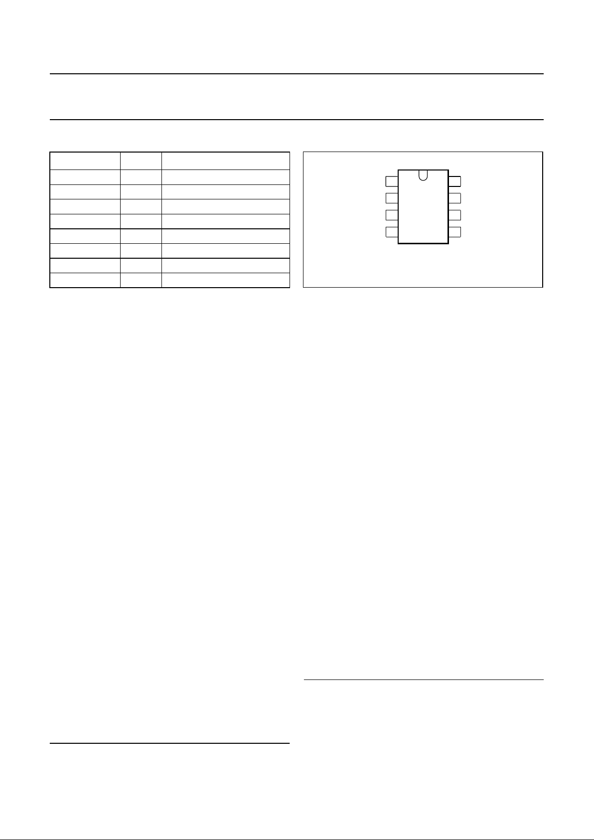
PCA1602T PMFP8 plastic micro flat package; 8 leads (straight) SOT144-1
PCA1603U/7 − chip with bumps on tape −
PCA1604U − chip in tray −
PCA1604U/10 − chip on foil −
PCA1605U/7 − chip with bumps on tape −
PCA1606U/10 − chip on foil −
PCA1607U − chip in tray −
PCA1608U − chip in tray −
PCA1611U − chip in tray −
PCA1621U/7 − chip with bumps on tape −
PCA1621U/10 − chip on foil −
PCA1622U − chip in tray −
PCA1623U/7 − chip with bumps on tape −
PCA1624U − chip in tray −
PCA1625U/7 − chip with bumps on tape −
PCA1626U − chip in tray −
PCA1627U/7 − chip with bumps on tape −
PCA1628U − chip in tray −
PCA1629U/7 − chip with bumps on tape −
1997 Dec 12 3
Philips Semiconductors Product specification
32 kHz watch circuits with EEPROM PCA16xx series
PINNING
SYMBOL PIN DESCRIPTION
V
SS
1 ground (0 V)
TEST 2 test output
OSC IN 3 oscillator input
OSC OUT 4 oscillator output
V
DD
5 positive supply voltage
M1 6 motor 1 output
M2 7 motor 2 output
RESET 8 reset input
Fig.1 Pin configuration, PCA16xxT, (PMFP8).
1
2
3
4
8
7
6
5
PCA16xxT
V
SS
TEST
OSC IN
OSC OUT
RESET
M2
M1
V
DD
MSA973
FUNCTIONAL DESCRIPTION AND TESTING
Motor pulse
The motor pulse width (t
P
) and the cycle times (tT) are
given in Chapter “Available types”.
Voltage level detector
The supply voltage is compared with the internal voltage
reference V
LIT
and V
EOL
every minute. The first voltage
level detection is carried out 30 ms after a RESET.
Lithium mode
If a lithium voltage is detected (V
DD
≥ V
LIT
), the circuit will
operate in the lithium mode. The motor pulse will be
produced with a 75% duty factor.
Silver-oxide mode
If the voltage level detected is between V
LIT
and V
EOL
, the
circuit will operate in silver-oxide mode.
Battery end-of-life
(1)
If the battery end-of-life is detected (VDD≤ V
EOL
), the
motor pulse will be produced without chopping. To indicate
this condition, bursts of 4 pulses are produced every 4 s.
Power-on reset
For correct operation of the Power-on reset the rise time of
V
DD
from 0 V to 2.1 V should be less than 0.1 ms.
All resettable flip-flops are reset. Additionally the polarity of
the first motor pulse is positive: VM1− VM2≥ 0V.
(1) Only available for types with a 1 s motor pulse.
Customer testing
An output frequency of 32 Hz is provided at RESET (pin 8)
to be used for exact frequency measurement. Every
minute a jitter occurs as a result of time calibration, which
occurs 90 to 150 ms after disconnecting the RESET from
VDD.
Connecting the RESET to VDD stops the motor pulses
leaving them in a HIGH impedance 3-state condition and a
32 Hz signal without jitter is produced at the TEST pin.
A debounce circuit protects accidental stoppages due to
mechanical shock to the watch (t
DEB
= 14.7 to 123.2 ms).
Connecting RESET to VSS activates Tests 1 and 2 and
disables the time calibration.
Test 1, VDD>V
EOL
. Normal function takes place except
the voltage detection cycle (tV) is 125 ms and the cycle
time tT1 is 31.25 ms. At pin TEST a minute signal is
available at 8192 times its normal frequency.
Test 2
(2)
, VDD<V
EOL
. The voltage detection cycle (tV) is
31.25 ms and the motor pulse period (tT2) = 31.25 ms.
Test and reset mode are terminated by disconnecting the
RESET pin.
Test 3, VDD> 5.1 V. Motor pulses with a time period of
tT3= 31.25 ms and n × 122 µs are produced to check the
contents of the EEPROM. At pin TEST the motor pulse
period signal (tT) is available at 1024 times its normal
frequency. The circuit returns to normal operation when
VDD< 2.5 V between two motor pulses.
(2) Only applicable for types with the battery end-of-life detector.
1997 Dec 12 4
Philips Semiconductors Product specification
32 kHz watch circuits with EEPROM PCA16xx series
Time calibration
Taking a normal quartz crystal with frequency 32768kHz,
frequency deviation (∆f/f) of ±15 × 10−6 and CL= 8.2 pF;
the oscillator frequency is offset (by using non-symmetrical
internal oscillator input and output capacitances of 10 pF
and 15 pF) such that the frequency deviation is
positive-only. This positive deviation can then be
compensated for to maintain time-keeping accuracy.
Once the positive frequency deviation is measured, a
corresponding number ‘n’ (see Table 1) is programmed
into the device’s EEPROM. This causes n pulses of
frequency 8192 Hz to be inhibited every minute of
operation, which achieves the required calibration.
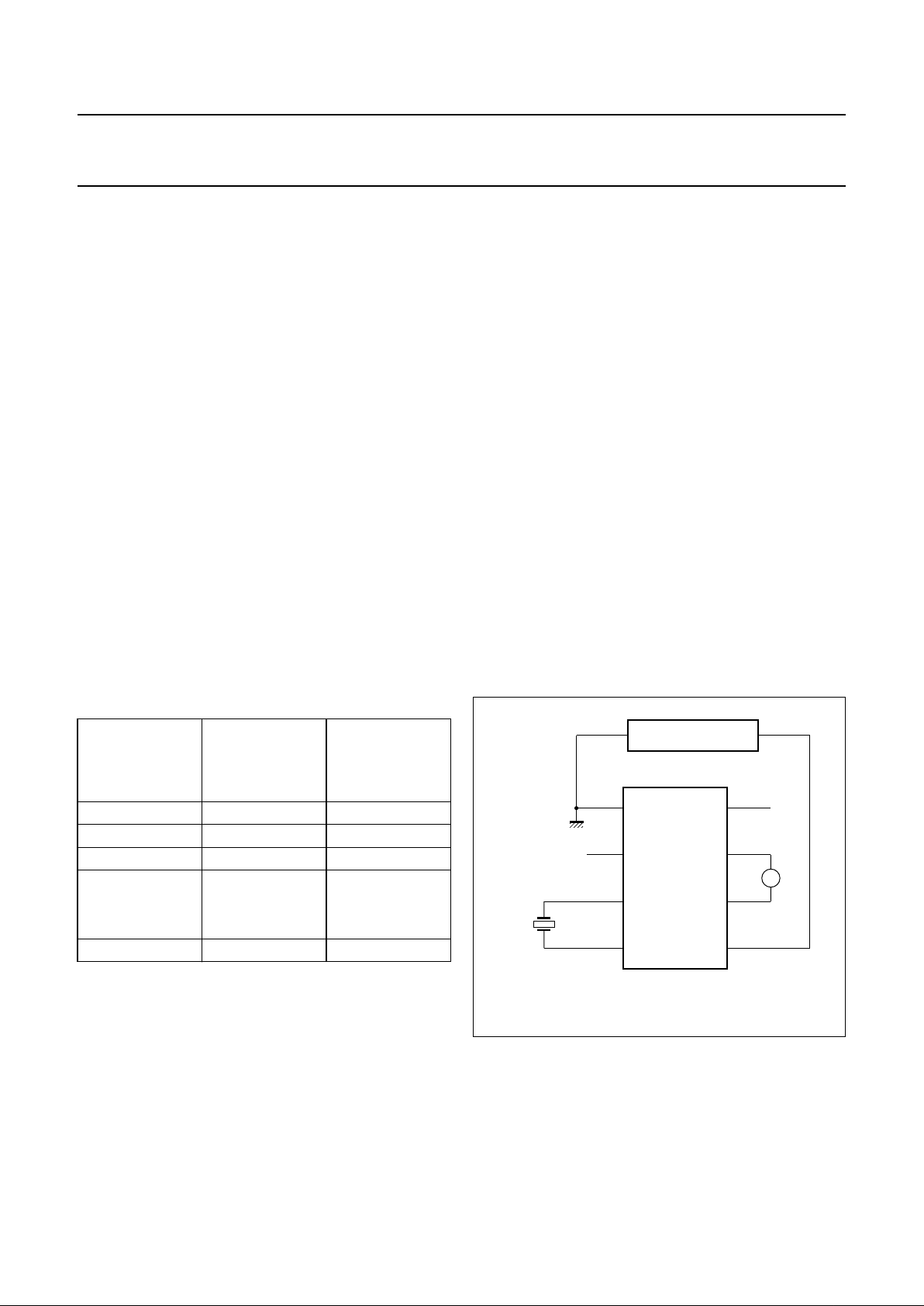
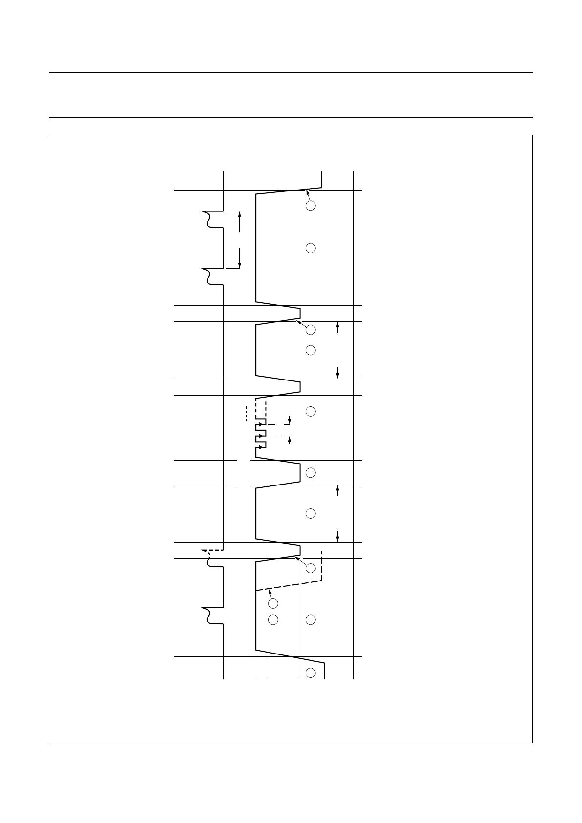
The programming circuit is shown in Fig.2. The required
number n is programmed into EEPROM by varying V
DD
according to the steps shown in Fig.3, which are
explained below:
1. The positive quartz frequency deviation (∆f/f) is
measured, and the corresponding values of n are
found according to Table 1.
2. VDD is increased to 5.1 V allowing the contents of the
EEPROM to be checked from the motor pulse period
tT3 at nominal frequency.
3. V
DD
is decreased to 2.5 V during a motor pulse to
initialize a storing sequence.
4. The first VDD pulse to 5.1 V erases the contents of
EEPROM.
5. When the EEPROM is erased a logic 1 is at the TEST
pin.
6. VDD is increased to 5.1 V to read the data by pulsing
VDD n times to 4.5 V. After the n edge, VDD is
decreased to 2.5 V.
7. VDD is increased to 5.1 V to store n bits in the
EEPROM.
8. VDD is decreased to 2.5 V to terminate the storing
sequence and to return to operating mode.
9. VDD is increased to 5.1 V to check writing from the
motor pulse period tT3.
10. VDD is decreased to the operation voltage between
two motor pulses to return to operating mode.
(Decreasing VDD during the motor pulse would restart
the programming mode).
The time calibration can be reprogrammed up to 100
times.
Table 1 Quartz crystal frequency deviation, n and t
T3
Notes
1. Increments of 2.03 × 10⁻⁶/step.
2. Increments of 122 µs/step.
FREQUENCY
DEVIATION
∆f/f
(× 10
−6
)
NUMBER OF
PULSES
(n)
t
T3
(ms)
0
(1)
0 31.250
(2)
+2.03 1 31.372
+4.06 2 31.494
...
...
...
+127.89 63 38.936
Fig.2 Circuit for programming the time calibration.
MSA975
V
DD
M1
M2
RESET
V
SS
TEST
OSC IN
OSC OUT
M
PCA16xx
SERIES
1
2
3
4
8
7
6
5
32 kHz
SIGNAL GENERATOR
1997 Dec 12 5
Philips Semiconductors Product specification
32 kHz watch circuits with EEPROM PCA16xx series
MSA948
∆ V
DDP
123 n
t = 1 µs
edge
0.1 ms
min.
t
T3
CHECKING
STORINGDATA INPUTERASURECONTENT CHECKING
1 2
9 10
3 4 5 6 7 8 9 10
I
DD
V (V)
DD
0 (V )
SS
2.5
1.5
4.5
5.1
(1) (1) (1) (1)
t = 5 ms
E
t = 5 ms
S
(1) Rise and fall time should be greater than 400 µs/V for immediately correct checking.
Fig.3 V
DD
for programming.
 Loading...