

Philips PBYR1645F, PBYR1645X, PBYR1640F, PBYR1640X Datasheet
Philips Semiconductors Product specification
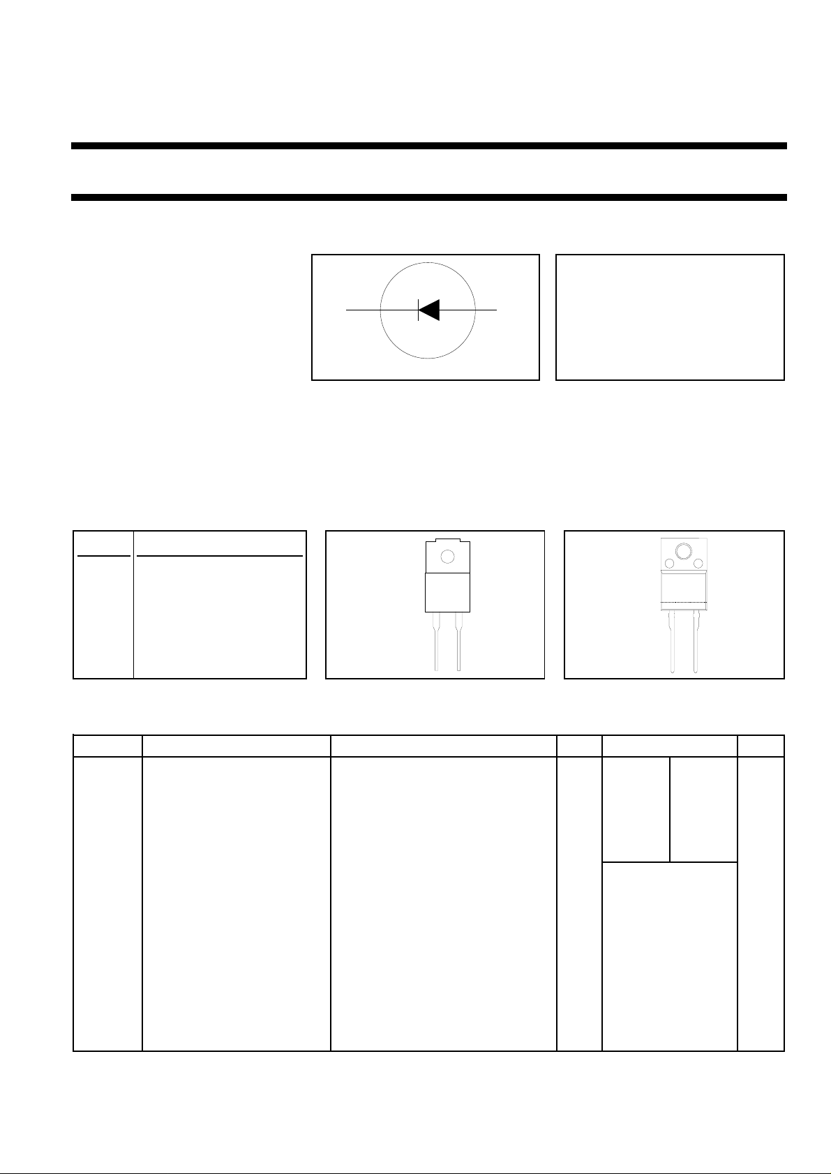
Rectifier diodes PBYR1645F, PBYR1645X
Schottky barrier
FEATURES SYMBOL QUICK REFERENCE DATA
• Low forward volt drop
• Fast switching V
• Reverse surge capability
• High thermal cycling performance I
k a
12
• Isolated mounting tab
GENERAL DESCRIPTION
Schottkyrectifierdiodesinaplasticenvelope withelectrically isolated mounting tab. Intended foruseasoutputrectifiers
in low voltage, high frequency switched mode power supplies.
The PBYR1645F is supplied in the SOD100 package.
The PBYR1645X is supplied in the SOD113 package.
PINNING SOD100 SOD113
= 40 V/ 45 V
R
= 16 A
F(AV)
VF ≤ 0.6 V
PIN DESCRIPTION
1 cathode
case
case
2 anode
tab isolated
12
12
LIMITING VALUES
Limiting values in accordance with the Absolute Maximum System (IEC 134)
SYMBOL PARAMETER CONDITIONS MIN. MAX. UNIT
PBYR16 40F 45F
V
V
V
I
F(AV)
I
FRM
I
FSM
I
RRM
T
T
RRM
RWM
R
j
stg
Peak repetitive reverse - 40 45 V
voltage
Working peak reverse - 40 45 V
voltage
Continuous reverse voltage Ths ≤ 97 ˚C - 40 45 V
Average rectified forward square wave; δ = 0.5; Ths ≤ 95 ˚C - 16 A
current
Repetitive peak forward square wave; δ = 0.5; Ths ≤ 95 ˚C - 32 A
current
Non-repetitive peak forward t = 10 ms - 120 A
current t = 8.3 ms - 132 A
sinusoidal; Tj = 125 ˚C prior to
surge; with reapplied V
Peak repetitive reverse pulse width and repetition rate - 1 A
surge current limited by T
j max
Operating junction - 150 ˚C
temperature
Storage temperature - 65 175 ˚C
PBYR16 40X 45X
RRM(max)
July 1998 1 Rev 1.200

Philips Semiconductors Product specification
Rectifier diodes PBYR1645F, PBYR1645X
Schottky barrier
ISOLATION LIMITING VALUE & CHARACTERISTIC
Ths = 25 ˚C unless otherwise specified
SYMBOL PARAMETER CONDITIONS MIN. TYP. MAX. UNIT
V
isol
V
isol
C
isol
THERMAL RESISTANCES
SYMBOL PARAMETER CONDITIONS MIN. TYP. MAX. UNIT
R
th j-hs
R
th j-a
Peak isolation voltage from SOD100 package; R.H. ≤ 65%; clean and - - 1500 V
both terminals to external dustfree
heatsink
R.M.S. isolation voltage from SOD113 package; f = 50-60 Hz; - - 2500 V
both terminals to external sinusoidal waveform; R.H. ≤ 65%; clean
heatsink and dustfree
Capacitance from pin 1 to f = 1 MHz - 10 - pF
external heatsink
Thermal resistance junction with heatsink compound - - 4.2 K/W
to heatsink
Thermal resistance junction in free air - 55 - K/W
to ambient
ELECTRICAL CHARACTERISTICS
Tj = 25 ˚C unless otherwise specified
SYMBOL PARAMETER CONDITIONS MIN. TYP. MAX. UNIT
V
F
I
R
C
d
Forward voltage IF = 16 A; Tj = 125˚C - 0.53 0.6 V
IF = 16 A - 0.55 0.68 V
Reverse current VR = V
Junction capacitance VR = 5 V; f = 1 MHz, Tj = 25˚C to 125˚C - 470 - pF
VR = V
RWM
; Tj = 100˚C - 27 40 mA
RWM
- 0.2 1.7 mA
July 1998 2 Rev 1.200
 Loading...