

Philips PBYR1035B, PBYR1040B, PBYR1045B Datasheet
Philips Semiconductors Product specification
Rectifier diodes PBYR1045B series
Schottky barrier
FEATURES SYMBOL QUICK REFERENCE DATA
• Low forward volt drop
• Fast switching V
• Reverse surge capability
• High thermal cycling performance I
k a
tab 3
• Low thermal resistance
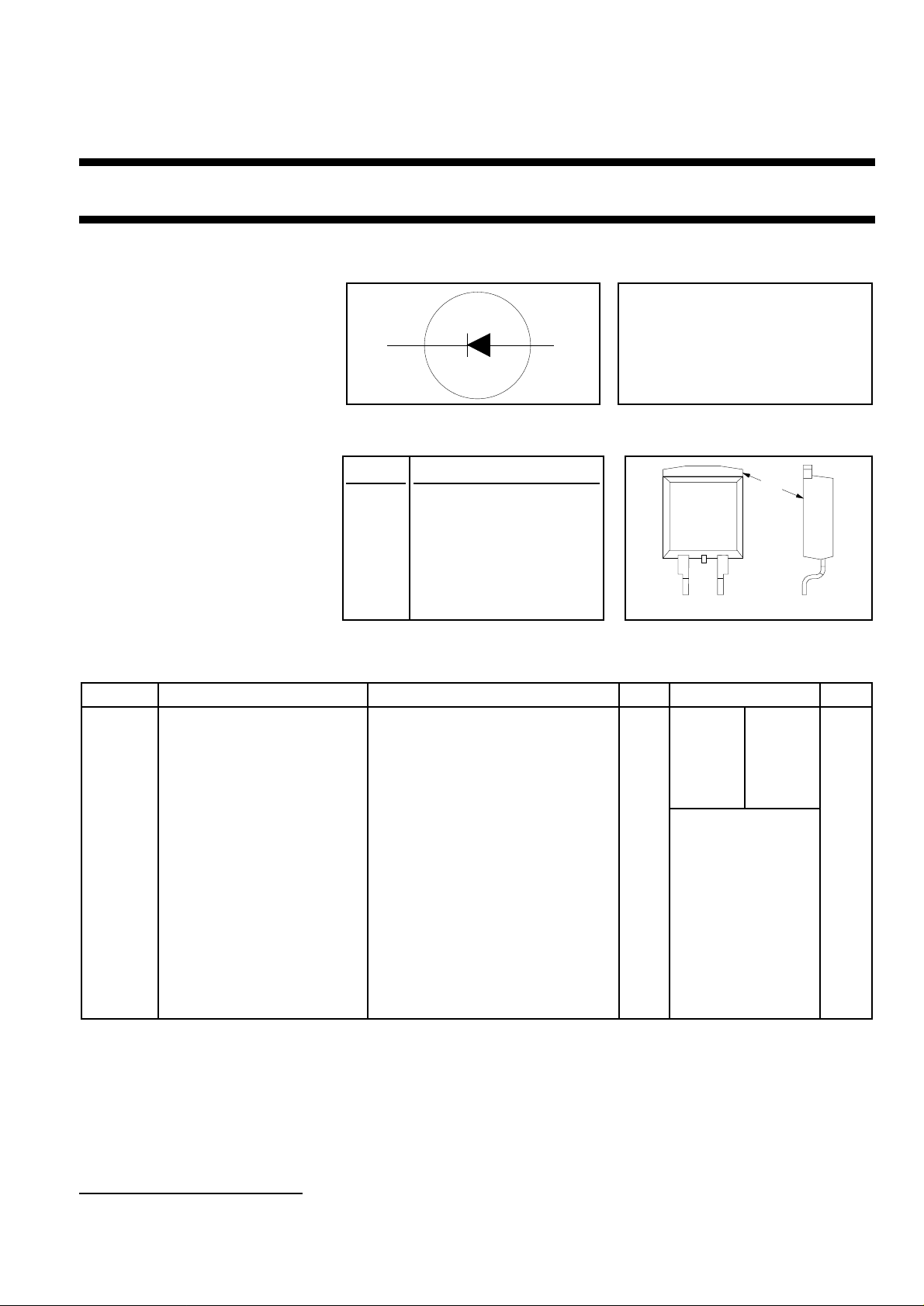
GENERAL DESCRIPTION PINNING SOT404
= 40 V/ 45 V
R
= 10 A
F(AV)
VF ≤ 0.57 V
Schottky rectifierdiodesin aplastic PIN DESCRIPTION
envelope. Intended for use as
mb
output rectifiersin low voltage, high 1 no connection
frequency switched mode power
supplies. 2 cathode
The PBYR1045B seriesissupplied 3 anode
in the surface mounting SOT404
package. tab cathode
1
2
13
LIMITING VALUES
Limiting values in accordance with the Absolute Maximum System (IEC 134)
SYMBOL PARAMETER CONDITIONS MIN. MAX. UNIT
V
V
V
I
F(AV)
I
FRM
I
FSM
I
RRM
T
T
RRM
RWM
R
j
stg
Peak repetitive reverse - 40 45 V
voltage
Working peak reverse - 40 45 V
voltage
Continuous reverse voltage Tmb ≤ 113 ˚C - 40 45 V
Average rectified forward square wave; δ = 0.5; Tmb ≤ 136 ˚C - 10 A
current
Repetitive peak forward square wave; δ = 0.5; Tmb ≤ 136 ˚C - 20 A
current
Non-repetitive peak forward t = 10 ms - 135 A
current t = 8.3 ms - 150 A
sinusoidal; Tj = 125 ˚C prior to
surge; with reapplied V
Peak repetitive reverse pulse width and repetition rate - 1 A
surge current limited by T
Operating junction - 150 ˚C
j max
temperature
Storage temperature - 65 175 ˚C
PBYR10 40B 45B
RRM(max)
1 It is not possible to make connection to pin 2 of the SOT404 package.
July 1998 1 Rev 1.200

Philips Semiconductors Product specification
Rectifier diodes PBYR1045B series
Schottky barrier
THERMAL RESISTANCES
SYMBOL PARAMETER CONDITIONS MIN. TYP. MAX. UNIT
R
th j-mb
R
th j-a
ELECTRICAL CHARACTERISTICS
Tj = 25 ˚C unless otherwise specified
SYMBOL PARAMETER CONDITIONS MIN. TYP. MAX. UNIT
V
F
I
R
C
d
Thermal resistance junction - - 2 K/W
to mounting base
Thermal resistance junction pcb mounted, minimum footprint, FR4 - 50 - K/W
to ambient board
Forward voltage IF = 10 A; Tj = 125˚C - 0.5 0.57 V
IF = 20 A; Tj = 125˚C - 0.69 0.72 V
IF = 20 A - 0.65 0.84 V
Reverse current VR = V
Junction capacitance VR = 5 V; f = 1 MHz, Tj = 25˚C to 125˚C - 350 - pF
VR = V
RWM
; Tj = 100˚C - 22 35 mA
RWM
- 0.2 1.3 mA
July 1998 2 Rev 1.200
 Loading...