

Philips PBSS9110T Technical data

查询PBSS9110T供应商
DISCRETE SEMICONDUCTORS
DATA SH EET
ook, halfpage
M3D088
PBSS9110T
100 V, 1 A
PNP low V
Product specification
Supersedes data of 2004 May 06
CEsat (BISS)
transistor
2004 May 13
Philips Semiconductors Product specification
100 V, 1 A
PNP low V
CEsat (BISS)
FEATURES
• SOT23 package
• Low collector-emitter saturation voltage V
• High collector current capability: IC and I
• Higher efficiency leading to less heat generation
APPLICATIONS
• Major application segments
– Automotive 42 V power
– Telecom infrastructure
– Industrial
• DC-to-DC conversion
• Peripheral drivers
– Driver in low supply voltage applications (e.g. lamps
and LEDs).
– Inductive load driver (e.g. relays,
buzzers and motors).
transistor
CEsat
CM
PBSS9110T
QUICK REFERENCE DATA
SYMBOL PARAMETER MAX. UNIT
V
CEO
I
C
I
CM
R
CEsat
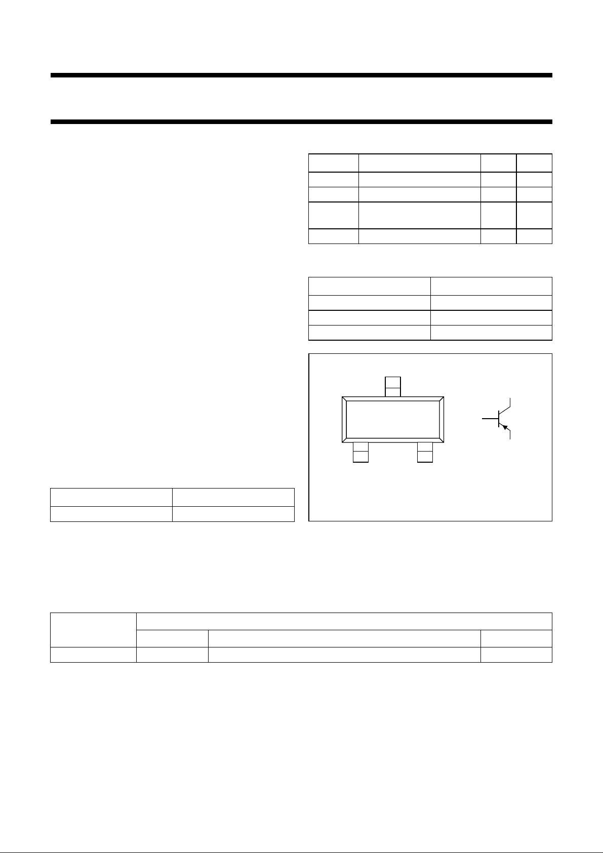
PINNING
handbook, halfpage
collector-emitter voltage −100 V
collector current (DC) −1A
repetitive peak collector
−3A
current
equivalent on-resistance 320 mΩ
PIN DESCRIPTION
1 base
2 emitter
3 collector
3
3
DESCRIPTION
PNP low V
transistor in a SOT23 plastic package.
CEsat
NPN complement: PBSS8110T.
MARKING
TYPE NUMBER MARKING CODE
21
Top view
(1)
Fig.1 Simplified outline (SOT23) and symbol.
1
2
MAM256
PBSS9110T *U7
Note
1. ∗ = p: Made in Hong Kong.
∗ = t: Made in Malaysia.
∗ = W: Made in China.
ORDERING INFORMATION
PACKAGE
TYPE NUMBER
NAME DESCRIPTION VERSION
PBSS9110T − plastic surface mounted package; 3 leads SOT23
2004 May 13 2
Philips Semiconductors Product specification
100 V, 1 A
PBSS9110T
PNP low V
CEsat (BISS)
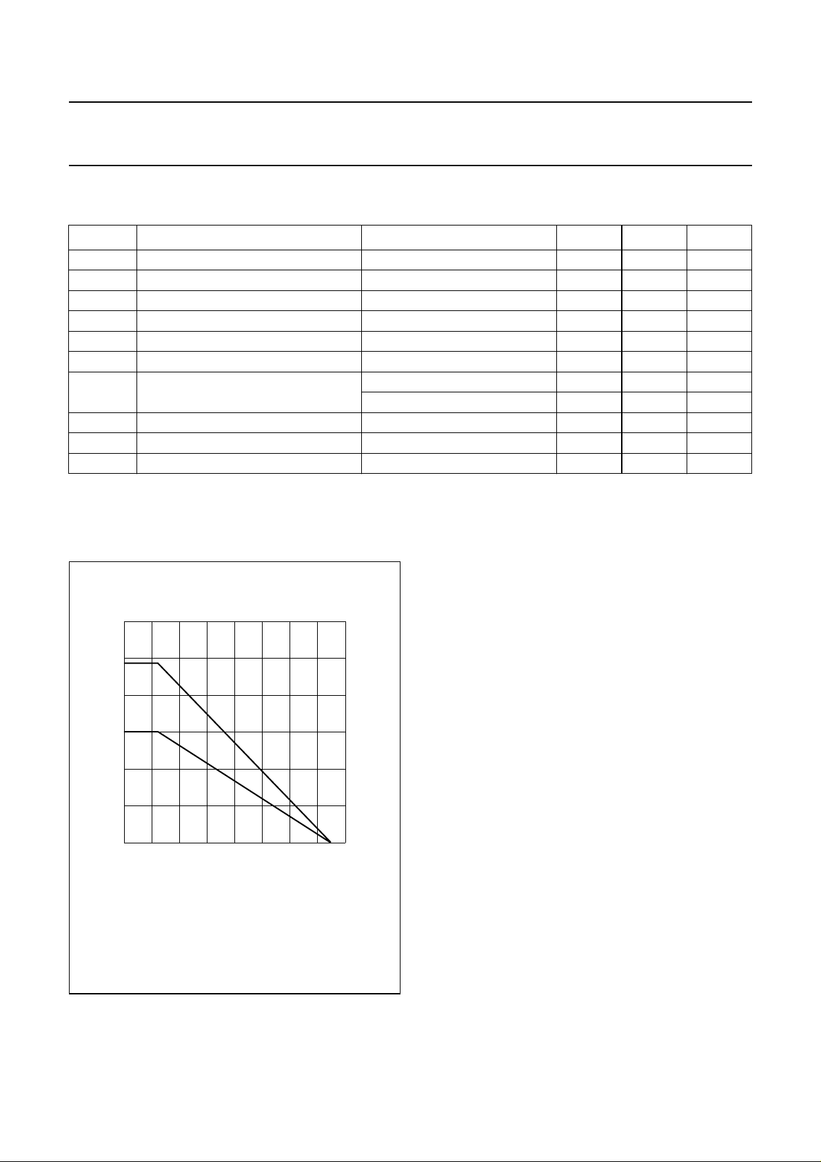
LIMITING VALUES
In accordance with the Absolute Maximum Rating System (IEC 60134).
SYMBOL PARAMETER CONDITIONS MIN. MAX. UNIT
V
V
V
I
I
I
P
T
T
T
CBO
CEO
EBO
C
CM
B
tot
j
amb
stg
collector-base voltage open emitter −−120 V
collector-emitter voltage open base −−100 V
emitter-base voltage open collector −−5V
collector current (DC) −−1A
peak collector current limited by T
base current (DC) −−300 mA
total power dissipation T
junction temperature − 150 °C
operating ambient temperature −65 +150 °C
storage temperature −65 +150 °C
Notes
1. Device mounted on a printed-circuit board, single-sided copper, tin-plated, standard footprint.
2. Device mounted on a printed-circuit board, single-sided copper, tin-plated and 1 cm2 collector mounting pad.
transistor
j(max)
≤ 25 °C; note 1 − 300 mW
amb
T
≤ 25 °C; note 2 − 480 mW
amb
−−3A
600
P
tot
(mW)
400
200
0
0
(1) 1 cm2 collector mounting pad.
(2) Standard footprint.
(1)
(2)
Fig.2 Power derating curves.
001aaa811
T
(°C)
amb
16012040 80
2004 May 13 3
Philips Semiconductors Product specification
100 V, 1 A
PBSS9110T
PNP low V
CEsat (BISS)
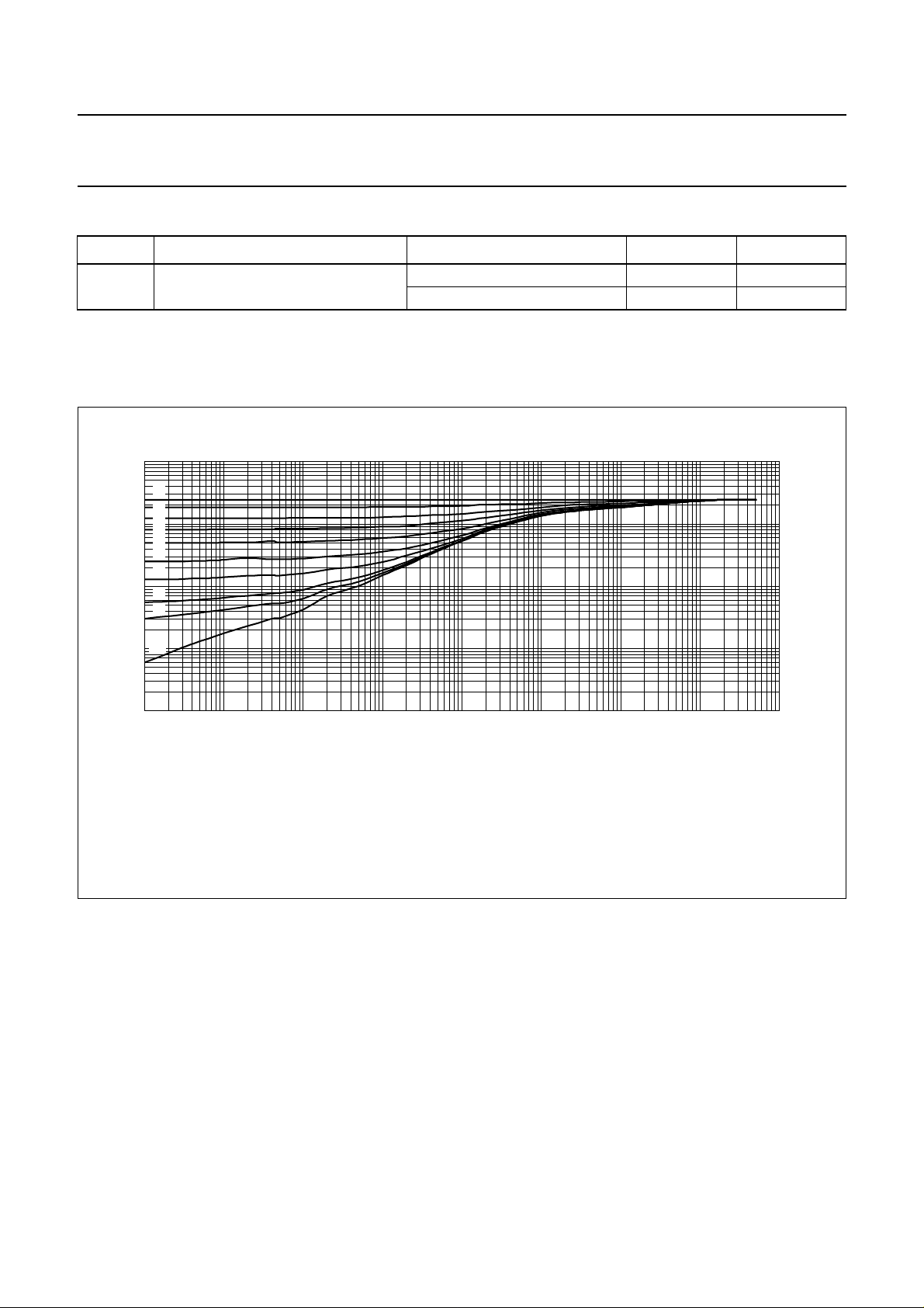
THERMAL CHARACTERISTICS
SYMBOL PARAMETER CONDITIONS VALUE UNIT
R
th(j-a)
thermal resistance from junction to
ambient
Notes
1. Device mounted on a printed-circuit board, single-sided copper, tin-plated and standard footprint.
2. Device mounted on a printed-circuit board, single-sided copper, tin-plated and 1 cm2 collector mounting pad.
3
10
Z
th
(K/W)
(1)
(2)
(3)
2
10
(4)
(5)
(6)
(7)
10
(8)
(9)
transistor
in free air; note 1 417 K/W
in free air; note 2 260 K/W
001aaa814
(10)
1
−1
10
−5
10
Mounted on printed-circuit board; 1 cm
(1) δ =1.
(2) δ = 0.75.
−4
10
(3) δ = 0.5.
(4) δ = 0.33.
Fig.3 Transient thermal impedance as a function of pulse time; typical values.
−3
10
2
collector mounting pad.
(5) δ = 0.2.
(6) δ = 0.1.
−2
−1
10
(7) δ = 0.05.
(8) δ = 0.02.
1
(9) δ = 0.01.
(10) δ =0.
1010
2
10
tp (s)
3
10
2004 May 13 4
 Loading...