


查询PBSS8110X-1供应商
PBSS8110X
100 V, 1 A NPN low V
Rev. 01 — 11 May 2005 Product data sheet
1. Product profile
1.1 General description
NPN low V
TO-243) SMD plastic package.
PNP complement: PBSS9110X.
1.2 Features
■ SOT89 package
■ Low collector-emitter saturation voltage V
■ High collector current capability: IC and I
■ High efficiency leading to less heat generation
1.3 Applications
(BISS) transistor
CEsat
Breakthrough in Small Signal (BISS) transistor in a SOT89 (SC-62/
CEsat
CEsat
CM
■ Major application segments:
◆ Automotive 42 V power
◆ Telecom infrastructure
◆ Industrial
■ Peripheral driver:
◆ Driver in low supply voltage applications (e.g. lamps and LEDs)
◆ Inductive load driver (e.g. relays, buzzers and motors)
■ DC-to-DC converter
1.4 Quick reference data
Table 1: Quick reference data
Symbol Parameter Conditions Min Typ Max Unit
V
CEO
I
C
I
CM
R
CEsat
[1] Pulse test: tp≤ 300 µs; δ≤ 0.02.
collector-emitter voltage open base - - 100 V
collector current (DC) - - 1 A
peak collector current single pulse;
t
≤ 1ms
p
collector-emitter
saturation resistance
IC=1A;
I
= 100 mA
B
--3 A
[1]
- 165 200 mΩ

Philips Semiconductors
PBSS8110X
2. Pinning information
Table 2: Pinning
Pin Description Simplified outline Symbol
1 emitter
2 collector
3 base
3. Ordering information
Table 3: Ordering information
Type number Package
PBSS8110X SC-62 plastic surface mounted package; collector pad for
100 V, 1 A NPN low V
321
Name Description Version
good heat transfer; 3 leads
(BISS) transistor
CEsat
3
sym042
2
1
SOT89
4. Marking
Table 4: Marking codes
Type number Marking code
PBSS8110X *4B
[1] * = -: made in Hong Kong
* = p: made in Hong Kong
* = t: made in Malaysia
* = W: made in China
[1]
9397 750 14956 © Koninklijke Philips Electronics N.V. 2005. All rights reserved.
Product data sheet Rev. 01 — 11 May 2005 2 of 15
Philips Semiconductors
PBSS8110X
5. Limiting values
Table 5: Limiting values
In accordance with the Absolute Maximum Rating System (IEC 60134).
Symbol Parameter Conditions Min Max Unit
V
CBO
V
CEO
V
EBO
I
C
I
CM
I
B
P
tot
T
j
T
amb
T
stg
[1] Device mounted on an FR4 Printed-Circuit Board (PCB), single-sided copper, tin-plated and standard
footprint.
[2] Device mounted on an FR4 PCB, single-sided copper, tin-plated, mounting pad for collector 6 cm2.
[3] Device mounted on a ceramic PCB, Al2O3, standard footprint.
100 V, 1 A NPN low V
(BISS) transistor
CEsat
collector-base voltage open emitter - 120 V
collector-emitter voltage open base - 100 V
emitter-base voltage open collector - 5 V
collector current (DC) - 1 A
peak collector current single pulse;
t
≤ 1ms
p
-3A
base current (DC) - 300 mA
total power dissipation T
amb
≤ 25 °C
[1]
- 0.55 W
[2]
- 1.4 W
[3]
- 2.0 W
junction temperature - 150 °C
ambient temperature −65 +150 °C
storage temperature −65 +150 °C
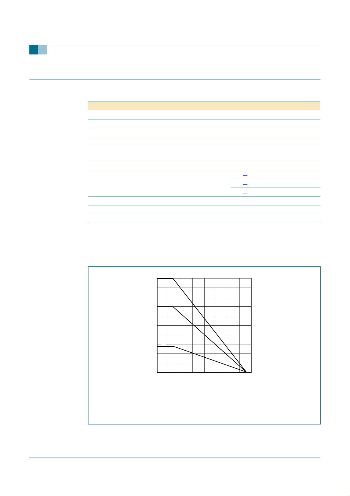
2.0
(1)
P
tot
(W)
1.6
(2)
1.2
0.8
(3)
0.4
0
0 16012040 80
(1) Ceramic PCB, Al2O3, standard footprint
(2) FR4 PCB; mounting pad for collector 6 cm
(3) FR4 PCB; standard footprint
Fig 1. Power derating curves
006aaa408
T
(°C)
amb
2
9397 750 14956 © Koninklijke Philips Electronics N.V. 2005. All rights reserved.
Product data sheet Rev. 01 — 11 May 2005 3 of 15
Philips Semiconductors
PBSS8110X
6. Thermal characteristics
Table 6: Thermal characteristics
Symbol Parameter Conditions Min Typ Max Unit
thermal resistance from
junction to ambient
thermal resistance from
junction to solder point
Z
th(j-a)
(K/W)
3
10
2
10
10
1
duty cycle =
1
0.75
0.5
0.33
0.2
0.1
0.05
0.02
0.01
0
R
th(j-a)
R
th(j-sp)
[1] Device mounted on an FR4 PCB, single-sided copper, tin-plated and standard footprint.
[2] Device mounted on an FR4 PCB, single-sided copper, tin-plated, mounting pad for collector 6 cm2.
[3] Device mounted on a ceramic PCB, Al2O3, standard footprint.
100 V, 1 A NPN low V
in free air
(BISS) transistor
CEsat
[1]
- - 227 K/W
[2]
--89K/W
[3]
--63K/W
--16K/W
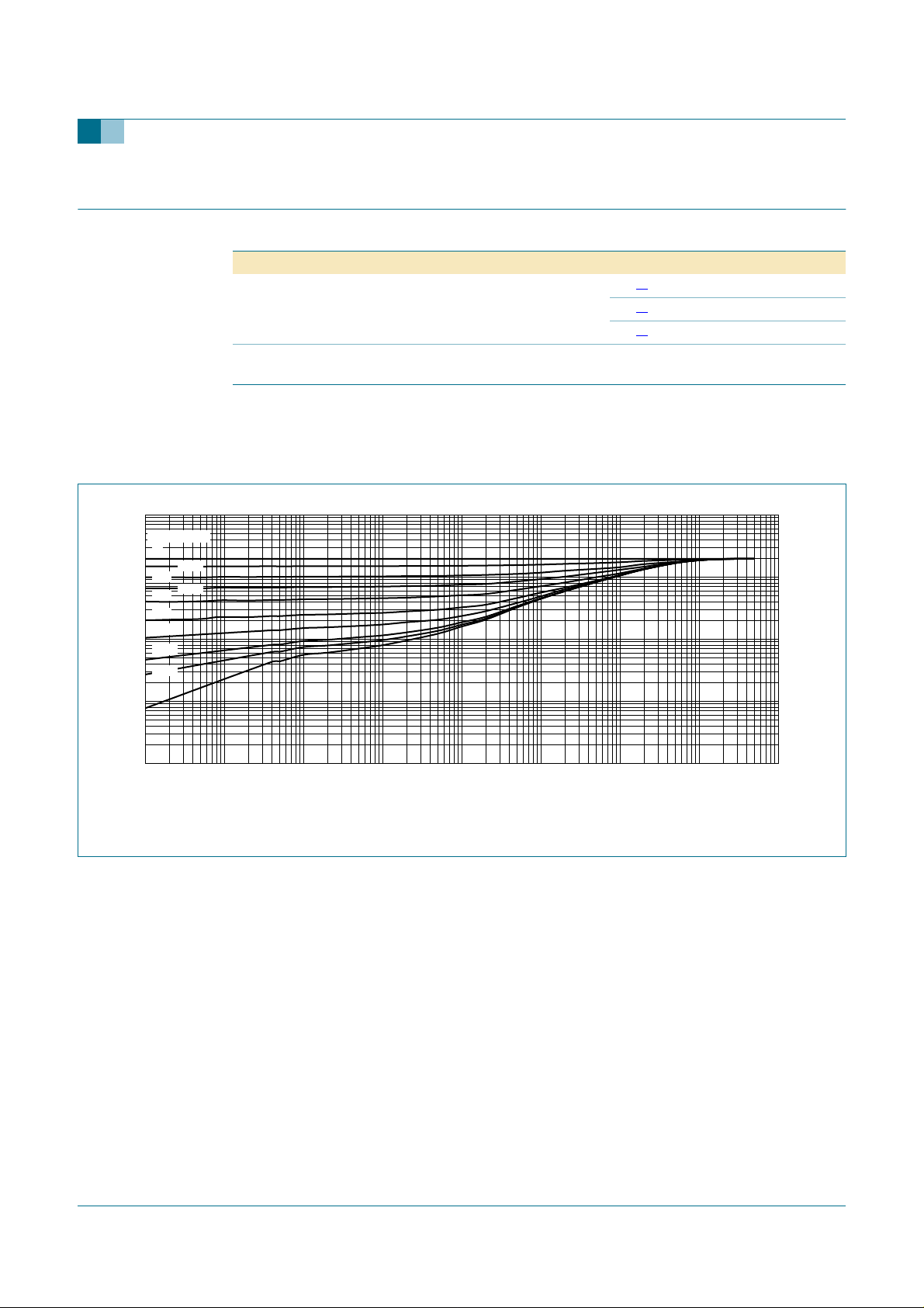
006aaa409
−1
10
−5
10
−4
10
−3
10
−2
−1
10
1
1010
2
10
tp (s)
3
10
FR4 PCB; standard footprint
Fig 2. Transient thermal impedance from junction to ambient as a function of pulse time; typical values
9397 750 14956 © Koninklijke Philips Electronics N.V. 2005. All rights reserved.
Product data sheet Rev. 01 — 11 May 2005 4 of 15

Philips Semiconductors
PBSS8110X
3
10
Z
th(j-a)
(K/W)
duty cycle =
2
10
1
0.75
0.5
0.33
0.2
0.1
10
0.05
0.02
0.01
1
0
−1
10
−5
10
−4
10
10
FR4 PCB; mounting pad for collector 6 cm
100 V, 1 A NPN low V
−3
−2
2
−1
10
1
1010
(BISS) transistor
CEsat
006aaa411
2
10
tp (s)
Fig 3. Transient thermal impedance from junction to ambient as a function of pulse time; typical values
10
Z
th(j-a)
(K/W)
2
duty cycle =
10
1
1
0.75
0.5
0.33
0.2
0.1
0.05
0.02
0.01
0
006aaa410
3
10
−1
10
−5
10
−4
10
−3
10
−2
−1
10
1
1010
2
10
tp (s)
3
10
Ceramic PCB, Al2O3, standard footprint
Fig 4. Transient thermal impedance from junction to ambient as a function of pulse time; typical values
9397 750 14956 © Koninklijke Philips Electronics N.V. 2005. All rights reserved.
Product data sheet Rev. 01 — 11 May 2005 5 of 15

Philips Semiconductors
PBSS8110X
100 V, 1 A NPN low V
(BISS) transistor
CEsat
7. Characteristics
Table 7: Characteristics
T
= 25°C unless otherwise specified.
amb
Symbol Parameter Conditions Min Typ Max Unit
I
CBO
I
CES
I
EBO
h
V
R
V
V
t
d
t
r
t
on
t
s
t
f
t
off
f
T
C
FE
CEsat
CEsat
BEsat
BEon
c
collector-base cut-off
current
collector-emitter
cut-off current
emitter-base cut-off
current
DC current gain VCE=10V; IC=1mA 150 - -
collector-emitter
saturation voltage
collector-emitter
saturation resistance
base-emitter
saturation voltage
base-emitter turn-on
voltage
delay time VCC=10V; IC= 0.5 A;
rise time - 220 - ns
turn-on time - 245 - ns
storage time - 365 - ns
fall time - 185 - ns
turn-off time - 550 - ns
transition frequency VCE=10V; IC=50mA;
collector capacitance VCB=10V; IE=ie=0A;
VCB=80V; IE= 0 A - - 100 nA
=80V; IE=0A;
V
CB
T
= 150 °C
j
--50µA
VCE=80V; VBE= 0 V - - 100 nA
VEB=4V; IC= 0 A - - 100 nA
=10V; IC= 250 mA 150 - 500
V
CE
=10V; IC= 500 mA
V
CE
=10V; IC=1A
V
CE
[1]
100 - -
[1]
80 - -
IC= 100 mA; IB=10mA --40mV
= 500 mA; IB= 50 mA - - 120 mV
I
C
= 1 A; IB= 100 mA
I
C
IC= 1 A; IB= 100 mA
[1]
- - 200 mV
[1]
- 165 200 mΩ
IC= 1 A; IB= 100 mA - - 1.05 V
VCE=10V; IC= 1 A - - 0.9 V
-25-ns
I
= 0.025 A; I
Bon
= −0.025 A
Boff
100 - - MHz
f = 100 MHz
- - 7.5 pF
f=1MHz
[1] Pulse test: tp≤ 300 µs; δ≤ 0.02.
9397 750 14956 © Koninklijke Philips Electronics N.V. 2005. All rights reserved.
Product data sheet Rev. 01 — 11 May 2005 6 of 15

Philips Semiconductors
PBSS8110X
600
h
FE
400
200
0
−1
10
110
(1)
(2)
(3)
10
2
001aaa497
3
10
I
C
(mA)
4
10
VCE =10V
(1) T
(2) T
(3) T
= 100 °C
amb
= 25 °C
amb
= −55 °C
amb
Fig 5. DC current gain as a function of collector
current; typical values
100 V, 1 A NPN low V
1000
V
BE
(mV)
800
600
400
200
−1
10
110
(1)
(2)
(3)
10
(BISS) transistor
CEsat
001aaa495
2
3
10
I
(mA)
C
4
10
VCE=10V
(1) T
(2) T
(3) T
= −55 °C
amb
= 25 °C
amb
= 100 °C
amb
Fig 6. Base-emitter voltage as a function of collector
current; typical values
001aaa504
3
10
IC (mA)
10
V
CEsat
(mV)
3
10
2
10
(1)
(2)
(3)
10
−1
10
110
10
2
IC/IB =10
(1) T
(2) T
(3) T
= 100 °C
amb
= 25 °C
amb
= −55 °C
amb
Fig 7. Collector-emitter saturation voltage as a
function of collector current; typical values
3
10
V
CEsat
(mV)
2
10
4
10
−1
10
IC/IB = 20; T
110
10
= 25 °C
amb
2
001aaa505
3
10
IC (mA)
4
10
Fig 8. Collector-emitter saturation voltage as a
function of collector current; typical values
9397 750 14956 © Koninklijke Philips Electronics N.V. 2005. All rights reserved.
Product data sheet Rev. 01 — 11 May 2005 7 of 15

Philips Semiconductors
PBSS8110X
001aaa506
3
10
I
C
(mA)
10
V
CEsat
(mV)
10
10
10
4
3
2
10
−1
10
IC/IB = 50; T
110
10
= 25 °CI
amb
2
Fig 9. Collector-emitter saturation voltage as a
function of collector current; typical values
100 V, 1 A NPN low V
1200
V
BEsat
(mV)
1000
(1)
800
600
400
4
200
(1) T
(2) T
(3) T
10
C/IB
amb
amb
amb
−1
110
=10
= −55 °C
= 25 °C
= 100 °C
(2)
(3)
10
(BISS) transistor
CEsat
001aaa498
2
3
10
I
(mA)
C
4
10
Fig 10. Base-emitter saturation voltageasafunctionof
collector current; typical values
001aaa499
3
10
I
C
(mA)
4
10
V
BEsat
(mV)
1200
1000
800
600
400
−1
10
IC/IB = 20; T
110
10
= 25 °CI
amb
2
Fig 11. Base-emitter saturation voltageasafunctionof
collector current; typical values
001aaa501
3
10
IC (mA)
(1)
(2)
(3)
4
10
R
CEsat
(Ω)
10
(1) T
(2) T
(3) T
3
10
2
10
10
1
−1
10
C/IB
amb
amb
amb
−1
110
10
=10
= 100 °C
= 25 °C
= −55 °C
2
Fig 12. Collector-emitter saturation resistance as a
function of collector current; typical values
9397 750 14956 © Koninklijke Philips Electronics N.V. 2005. All rights reserved.
Product data sheet Rev. 01 — 11 May 2005 8 of 15

Philips Semiconductors
PBSS8110X
001aaa502
3
10
IC (mA)
4
10
R
10
CEsat
(Ω)
10
10
3
2
10
1
−1
−1
10
IC/IB = 20; T
110
10
= 25 °CI
amb
2
Fig 13. Collector-emitter saturation resistance as a
function of collector current; typical values
100 V, 1 A NPN low V
3
10
R
CEsat
(Ω)
2
10
10
1
−1
10
−1
10
C/IB
110
= 50; T
amb
10
= 25 °C
(BISS) transistor
CEsat
001aaa503
10
3
IC (mA)
2
4
10
Fig 14. Collector-emitter saturation resistance as a
function of collector current; typical values
001aaa496
VCE (V)
T
amb
= 25 °C
(A)
I
C
1.6
1.2
0.8
0.4
2
0
054231
(1)
(2)
(3)
(4)
(5)
(6)
(7)
(8)
(9)
(10)
(1) IB = 35 mA
(2) IB = 31.5 mA
(3) IB = 28 mA
(4) IB = 24.5 mA
(5) IB = 21 mA
(6) IB = 17.5 mA
(7) IB = 14 mA
(8) IB = 10.5 mA
(9) IB = 7 mA
(10) IB = 3.5 mA
Fig 15. Collector current as a function of collector-emitter voltage; typical values
9397 750 14956 © Koninklijke Philips Electronics N.V. 2005. All rights reserved.
Product data sheet Rev. 01 — 11 May 2005 9 of 15

Philips Semiconductors
PBSS8110X
8. Test information
90 %
10 %
90 %
100 V, 1 A NPN low V
I
B
I
(100 %)
Bon
I
Boff
I
C
(BISS) transistor
CEsat
input pulse
(idealized waveform)
output pulse
(idealized waveform)
10 %
t
t
d
r
t
on
Fig 16. BISS transistor switching time definition
V
BB
R
R1
R2
B
= −0.025 A
Boff
oscilloscope
V
I
VCC=10V; IC= 0.5 A; I
(probe)
450 Ω
= 0.025 A; I
Bon
Fig 17. Test circuit for switching times
IC (100 %)
t
t
s
t
off
V
CC
R
C
V
o
(probe)
oscilloscope
450 Ω
DUT
mlb826
t
f
006aaa003
9397 750 14956 © Koninklijke Philips Electronics N.V. 2005. All rights reserved.
Product data sheet Rev. 01 — 11 May 2005 10 of 15

Philips Semiconductors
PBSS8110X
9. Package outline
Fig 18. Package outline SOT89 (SC-62/TO-243)
2.6
2.4
100 V, 1 A NPN low V
4.6
4.4
1.8
1.4
123
0.53
0.40
1.5
3
0.48
0.35
1.2
0.8
1.6
1.4
4.25
3.75
0.44
0.23
04-08-03Dimensions in mm
(BISS) transistor
CEsat
10. Packing information
Table 8: Packing methods
The indicated -xxx are the last three digits of the 12NC ordering code.
Type number Package Description Packing quantity
PBSS8110X SOT89 8 mm pitch, 12 mm tape and reel -115 -135
[1] For further information and the availability of packing methods, seeSection18.
[1]
1000 4000
9397 750 14956 © Koninklijke Philips Electronics N.V. 2005. All rights reserved.
Product data sheet Rev. 01 — 11 May 2005 11 of 15

Philips Semiconductors
PBSS8110X
11. Soldering
4.60
0.85
0.20
1.20
1.20
1.00
(3x)
4.75
2.25
2.00
1.90
1.20
3.70
3.95
100 V, 1 A NPN low V
1.70
0.50
132
0.60 (3x)
0.70 (3x)
4.85
1.20
msa442
(BISS) transistor
CEsat
solder lands
solder resist
occupied area
solder paste
12. Mounting
Reflow soldering is the only recommended soldering method.
Dimensions in mm
Fig 19. Reflow soldering footprint SOT89 (SC-62/TO-243)
32 mm
40
mm
2.5 mm
2.5 mm
0.5 mm
3.96 mm
1 mm
3 mm
1 mm
1.6 mm
001aaa234
40
mm
5 mm
2.5 mm
0.5 mm
3.96 mm
32 mm
30 mm
20
mm
1 mm
5 mm
1.6 mm
001aaa235
Fig 20. FR4 PCB, standard footprint Fig 21. FR4 PCB, mounting pad for
collector 6 cm
9397 750 14956 © Koninklijke Philips Electronics N.V. 2005. All rights reserved.
Product data sheet Rev. 01 — 11 May 2005 12 of 15
2

Philips Semiconductors
PBSS8110X
100 V, 1 A NPN low V
(BISS) transistor
CEsat
13. Revision history
Table 9: Revision history
Document ID Release date Data sheet status Change notice Doc. number Supersedes
PBSS8110X_1 20050511 Product data sheet - 9397 750 14956 -
9397 750 14956 © Koninklijke Philips Electronics N.V. 2005. All rights reserved.
Product data sheet Rev. 01 — 11 May 2005 13 of 15

Philips Semiconductors
PBSS8110X
100 V, 1 A NPN low V
(BISS) transistor
CEsat
14. Data sheet status
Level Data sheet status
I Objective data Development This data sheet contains data from the objective specification for product development. Philips
II Preliminary data Qualification This data sheet contains data from the preliminary specification. Supplementary data will be published
III Product data Production This data sheet contains data from the product specification. Philips Semiconductors reserves the
[1] Please consult the most recently issued data sheet before initiating or completing a design.
[2] The product status of the device(s) described in this data sheet may have changed since this data sheet was published. The latest information is available on the Internet at
URL http://www.semiconductors.philips.com.
[3] For data sheets describing multiple type numbers, the highest-level product status determines the data sheet status.
[1]
Product status
15. Definitions
Short-form specification — The data in a short-form specification is
extracted from a full data sheet with the same type number and title. For
detailed information see the relevant data sheet or data handbook.
Limiting values definition — Limiting values given are in accordance with
the Absolute Maximum Rating System (IEC 60134). Stress above one or
more of the limiting values may cause permanent damage to the device.
These are stress ratings only and operation of the device at these or at any
other conditions above those given in the Characteristics sections of the
specification is not implied. Exposure to limiting values for extended periods
may affect device reliability.
Application information — Applications that are described herein for any
of these products are for illustrative purposes only. Philips Semiconductors
make no representation or warranty that such applications will be suitable for
the specified use without further testing or modification.
[2] [3]
Definition
Semiconductors reserves the right to change the specification in any manner without notice.
at a later date. Philips Semiconductors reserves the right to change the specification without notice, in
order to improve the design and supply the best possible product.
right to make changes at any time in order to improve the design, manufacturing and supply. Relevant
changes will be communicated via a Customer Product/Process Change Notification (CPCN).
customers using or selling these products for use in such applications do so
at their own risk and agree to fully indemnify Philips Semiconductors for any
damages resulting from such application.
Right to make changes — Philips Semiconductors reserves the right to
make changes in the products - including circuits, standard cells, and/or
software - described or contained herein in order to improve design and/or
performance. When the product is in full production (status ‘Production’),
relevant changes will be communicated via a Customer Product/Process
Change Notification (CPCN). Philips Semiconductors assumes no
responsibility or liability for the use of any of these products, conveys no
license or title under any patent, copyright, or mask work right to these
products, and makes no representations or warranties that these products are
free from patent, copyright, or mask work right infringement, unless otherwise
specified.
17. Trademarks
16. Disclaimers
Life support — These products are not designed for use in life support
appliances, devices, or systems where malfunction of these products can
reasonably be expected to result in personal injury. Philips Semiconductors
Notice — All referenced brands, product names, service names and
trademarks are the property of their respective owners.
18. Contact information
For additional information, please visit: http://www.semiconductors.philips.com
For sales office addresses, send an email to: sales.addresses@www.semiconductors.philips.com
9397 750 14956 © Koninklijke Philips Electronics N.V. 2005. All rights reserved.
Product data sheet Rev. 01 — 11 May 2005 14 of 15

Philips Semiconductors
PBSS8110X
19. Contents
1 Product profile . . . . . . . . . . . . . . . . . . . . . . . . . . 1
1.1 General description. . . . . . . . . . . . . . . . . . . . . . 1
1.2 Features . . . . . . . . . . . . . . . . . . . . . . . . . . . . . . 1
1.3 Applications . . . . . . . . . . . . . . . . . . . . . . . . . . . 1
1.4 Quick reference data. . . . . . . . . . . . . . . . . . . . . 1
2 Pinning information. . . . . . . . . . . . . . . . . . . . . . 2
3 Ordering information. . . . . . . . . . . . . . . . . . . . . 2
4 Marking. . . . . . . . . . . . . . . . . . . . . . . . . . . . . . . . 2
5 Limiting values. . . . . . . . . . . . . . . . . . . . . . . . . . 3
6 Thermal characteristics. . . . . . . . . . . . . . . . . . . 4
7 Characteristics. . . . . . . . . . . . . . . . . . . . . . . . . . 6
8 Test information. . . . . . . . . . . . . . . . . . . . . . . . 10
9 Package outline . . . . . . . . . . . . . . . . . . . . . . . . 11
10 Packing information. . . . . . . . . . . . . . . . . . . . . 11
11 Soldering . . . . . . . . . . . . . . . . . . . . . . . . . . . . . 12
12 Mounting. . . . . . . . . . . . . . . . . . . . . . . . . . . . . . 12
13 Revision history. . . . . . . . . . . . . . . . . . . . . . . . 13
14 Data sheet status. . . . . . . . . . . . . . . . . . . . . . . 14
15 Definitions . . . . . . . . . . . . . . . . . . . . . . . . . . . . 14
16 Disclaimers. . . . . . . . . . . . . . . . . . . . . . . . . . . . 14
17 Trademarks. . . . . . . . . . . . . . . . . . . . . . . . . . . . 14
18 Contact information . . . . . . . . . . . . . . . . . . . . 14
100 V, 1 A NPN low V
(BISS) transistor
CEsat
© Koninklijke Philips Electronics N.V. 2005
All rights are reserved. Reproduction in whole or in part is prohibited without the prior
written consent of the copyright owner. The information presented in this document does
not form part of any quotation or contract, is believed to be accurate and reliable and may
be changed without notice. No liability will be accepted by the publisher for any
consequence of its use. Publication thereof does not convey nor imply any license under
patent- or other industrial or intellectual property rights.
Published in The Netherlands
Date of release: 11 May 2005
Document number: 9397 750 14956
 Loading...