


查询PBSS5540X供应商
DISCRETE SEMICONDUCTORS
DATA SH EET
ook, halfpage
M3D109
PBSS5540X
40 V, 5 A
PNP low V
Product specification
Supersedes data of 2004 Jan 15
CEsat
(BISS) transistor
2004 Nov 04
Philips Semiconductors Product specification
40 V, 5 A
PNP low V
CEsat
FEATURES
• Low collector-emitter saturation voltage V
• High collector current capability: IC and I
• High efficiency leading to less heat generation.
APPLICATIONS
• Supply line switching circuits
• Battery management applications
• DC/DC converter applications
• Strobe flash units
• Medium power driver (e.g. relays, buzzers and motors).
DESCRIPTION
PNP low V
transistor in a medium power SOT89
CEsat
(SC-62) package.
NPN complement: PBSS4540X.
(BISS) transistor
CEsat
CM
PBSS5540X
QUICK REFERENCE DATA
SYMBOL PARAMETER MAX. UNIT
V
CEO
I
C
I
CRP
R
CEsat
PINNING
PIN DESCRIPTION
1 emitter
2 collector
3 base
collector-emitter voltage −40 V
collector current (DC) −4A
repetitive peak collector
−5A
current
equivalent
75 mΩ
on-resistance
MARKING
TYPE NUMBER MARKING CODE
(1)
PBSS5540X *1G
Note
1. * = p: Made in Hong Kong.
321
* = t: Made in Malaysia.
* = W: Made in China.
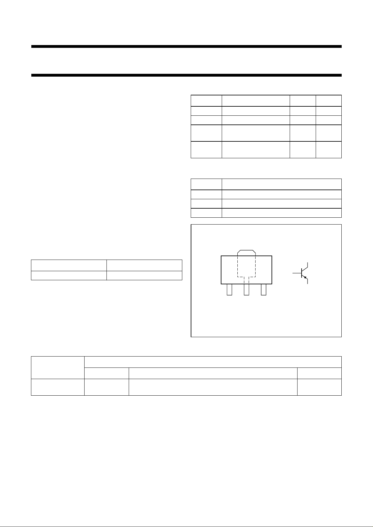
Fig.1 Simplified outline (SOT89) and symbol.
ORDERING INFORMATION
PACKAGE
TYPE NUMBER
NAME DESCRIPTION VERSION
PBSS5540X SC-62 plastic surface mounted package; collector pad for good heat
transfer; 3 leads
2
3
1
sym079
SOT89
2004 Nov 04 2

Philips Semiconductors Product specification
40 V, 5 A
PBSS5540X
PNP low V
LIMITING VALUES
In accordance with the Absolute Maximum Rating System (IEC 60134).
SYMBOL PARAMETER CONDITIONS MIN. MAX. UNIT
V
V
V
I
CM
I
CRP
I
C
I
BM
I
B
P
T
T
T
CBO
CEO
EBO
tot
stg
j
amb
collector-base voltage open emitter −−40 V
collector-emitter voltage open base −−40 V
emitter-base voltage open collector −−6V
peak collector current tp≤ 1ms −−10 A
repetitive peak collector current tp≤ 10 ms; δ≤0.2 −−5A
collector current (DC) −−4A
peak base current tp≤ 1ms −−2A
base current (DC) −−1A
total power dissipation T
storage temperature −65 +150 °C
junction temperature − 150 °C
ambient temperature −65 +150 °C
(BISS) transistor
CEsat
≤ 25 °C
amb
tp≤ 10 ms; δ≤0.2; note 1 − 2.5 W
note 1 − 0.55 W
note 2 − 1W
note 3 − 1.4 W
note 4 − 1.6 W
Notes
1. Device mounted on a printed-circuit board, single-sided copper, tin-plated and standard footprint.
2. Device mounted on a printed-circuit board, single-sided copper, tin-plated and mounting pad for collector 1 cm2.
3. Device mounted on a printed-circuit board, single-sided copper, tin-plated and mounting pad for collector 6 cm2.
4. Device mounted on a 7 cm2 ceramic printed-circuit board, 1 cm2 single-sided copper and tin-plated.
2004 Nov 04 3
Philips Semiconductors Product specification
40 V, 5 A
PNP low V
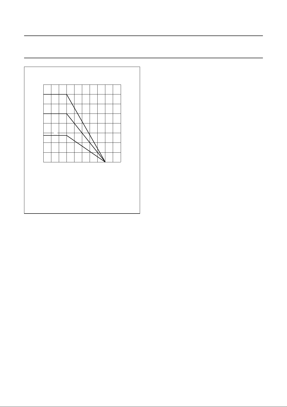
1600
P
tot
(mW)
1200
800
400
(1) FR4 PCB; 6 cm2 mounting pad for collector.
(2) FR4 PCB; 1 cm2 mounting pad for collector.
(3) FR4 PCB; standard footprint.
(1)
(2)
(3)
0
−50 20015050 1000
(BISS) transistor
CEsat
001aaa229
T
(°C)
amb
PBSS5540X
Fig.2 Power derating curves.
2004 Nov 04 4

Philips Semiconductors Product specification
40 V, 5 A
PBSS5540X
PNP low V
THERMAL CHARACTERISTICS
SYMBOL PARAMETER CONDITIONS VALUE UNIT
R
th(j-a)
R
th(j-s)
Notes
1. Pulse test: tp≤ 10 ms; δ≤0.2.
2. Device mounted on a printed-circuit board, single-sided copper, tin-plated and standard footprint.
3. Device mounted on a printed-circuit board, single-sided copper, tin-plated and mounting pad for collector 1 cm2.
4. Device mounted on a printed-circuit board, single-sided copper, tin-plated and mounting pad for collector 6 cm2.
5. Device mounted on a 7 cm2 ceramic printed-circuit board, 1 cm2 single-sided copper and tin-plated.
thermal resistance from junction to
ambient
thermal resistance from junction to
soldering point
(BISS) transistor
CEsat
in free air
notes 1 and 2 50 K/W
note 2 225 K/W
note 3 125 K/W
note 4 90 K/W
note 5 80 K/W
16 K/W
3
10
Z
th
(K/W)
2
10
10
1
−1
10
−5
10
Mounted on FR4 printed-circuit board; standard footprint.
(1) δ =1.
(2) δ = 0.75.
(1)
(2)
(3)
(4)
(5)
(6)
(7)
(8)
(9)
(10)
−4
10
(3) δ = 0.5.
(4) δ = 0.33.
−3
10
(5) δ = 0.2.
(6) δ = 0.1.
Fig.3 Transient thermal impedance as a function of pulse time; typical values.
−2
−1
10
(7) δ = 0.05.
(8) δ = 0.02.
1
(9) δ = 0.01.
(10) δ =0.
006aaa232
1010
2
10
tp (s)
3
10
2004 Nov 04 5

Philips Semiconductors Product specification
40 V, 5 A
PNP low V
3
10
Z
th
(K/W)
Mounted on FR4 printed-circuit board; mounting pad for collector 1 cm2.
(1)
2
10
10
(2)
(3)
(4)
(5)
(6)
(7)
(8)
(9)
1
(10)
−1
10
−5
10
(BISS) transistor
CEsat
−4
10
−3
10
−2
PBSS5540X
006aaa233
−1
10
1
1010
2
10
tp (s)
3
10
(1) δ =1.
(2) δ = 0.75.
3
10
Z
th
(K/W)
2
10
10
1
−1
10
−5
10
(1)
(3)
(5)
(6)
(7)
(8)
(9)
(10)
(3) δ = 0.5.
(4) δ = 0.33.
(5) δ = 0.2.
(6) δ = 0.1.
(7) δ = 0.05.
(8) δ = 0.02.
(9) δ = 0.01.
(10) δ =0.
Fig.4 Transient thermal impedance as a function of pulse time; typical values.
(2)
(4)
−4
10
−3
10
−2
−1
10
1
1010
006aaa234
2
10
tp (s)
3
10
Mounted on FR4 printed-circuit board; mounting pad for collector 6 cm2.
(1) δ =1.
(2) δ = 0.75.
(3) δ = 0.5.
(4) δ = 0.33.
(5) δ = 0.2.
(6) δ = 0.1.
(7) δ = 0.05.
(8) δ = 0.02.
Fig.5 Transient thermal impedance as a function of pulse time; typical values.
2004 Nov 04 6
(9) δ = 0.01.
(10) δ =0.

Philips Semiconductors Product specification
40 V, 5 A
PBSS5540X
PNP low V
CHARACTERISTICS
T
=25°C unless otherwise specified.
amb
SYMBOL PARAMETER CONDITIONS MIN. TYP. MAX. UNIT
I
CBO
I
EBO
h
V
R
V
V
f
T
C
FE
CEsat
CEsat
BEsat
BEon
c
collector-base cut-off current VCB= −30 V; IE=0A −−−100 nA
emitter-base cut-off current VEB= −5 V; IC=0A −−−100 nA
DC current gain VCE= −2 V; IC= −0.5 A 250 −−
collector-emitter saturation
voltage
equivalent on-resistance IC= −5 A; IB= −500 mA;
base-emitter saturation
voltage
base-emitter turn-on voltage VCE= −2 V; IC= −2A −−−1.0 V
transition frequency VCE= −10 V; IC= −0.1 A;
collector capacitance VCB= −10 V; IE= ie=0A;
(BISS) transistor
CEsat
= −30 V; IE=0A;
V
CB
T
= 150 °C
j
VCE= −2 V; IC= −1A;
−−−50 µA
200 −−
note 1
VCE= −2 V; IC= −2A;
150 −−
note 1
VCE= −2 V; IC= −5A;
50 −−
note 1
IC= −0.5 A; IB= −5mA −−120 mV
IC= −1 A; IB= −10 mA −−170 mV
IC= −2 A; IB= −200 mA −−160 mV
IC= −4 A; IB= −200 mA;
−−340 mV
note 1
IC= −5 A; IB= −500 mA;
−−375 mV
note 1
− 45 75 mΩ
note 1
IC= −4 A; IB= −200 mA;
−−−1.1 V
note 1
IC= −5 A; IB= −500 mA;
−−−1.2 V
note 1
60 −−MHz
f = 100 MHz
−−105 pF
f = 1 MHz
Note
1. Pulse test: t
≤ 300 µs; δ≤0.02.
p
2004 Nov 04 7

Philips Semiconductors Product specification
40 V, 5 A
PNP low V
−8
I
C
(A)
−6
−4
−2
0
0 −2−1.5−0.5 −1
(1) IB1= −11 mA.
(2) IB2= −22 mA.
(3) IB3= −33 mA.
(BISS) transistor
CEsat
(1)
(2)
(3)
(4)
(5)
(4) IB4= −44 mA.
(5) IB5= −55 mA.
001aaa157
V
(V)
CE
−1.2
V
BE
(V)
−0.8
−0.4
V
CE
(1) T
0
−1
−10
= −2V.
= −55 °C. (2) T
amb
−1 −10
−10
=25°C. (3) T
amb
PBSS5540X
001aaa158
(1)
(2)
(3)
−10
3
I
C
(mA)
amb
−10
2
4
= 100 °C.
Fig.6 Collector current as a function of
collector-emitter voltage; typical values.
1000
h
FE
800
600
400
200
0
−1
−10
VCE= −2V.
(1) T
amb
−1 −10
−10
= 100 °C. (2) T
(1)
(2)
(3)
=25°C. (3) T
amb
001aaa159
−10
3
I
2
(mA)
C
amb
4
−10
= −55 °C.
Fig.7 Base-emitter voltage as a function of
collector current; typical values.
001aaa160
(1)
(3)
−10
3
IC (mA)
amb
2
R
CEsat
(Ω)
10
10
I
C/IB
(1) T
2
10
10
1
−1
−2
−1
−10
= 20.
= 100 °C. (2) T
amb
(2)
−1 −10
−10
=25°C. (3) T
amb
4
−10
= −55 °C.
Fig.8 DC current gain as a function of collector
current; typical values.
2004 Nov 04 8
Fig.9 Equivalent on-resistance as a function of
collector current; typical values.

Philips Semiconductors Product specification
40 V, 5 A
PNP low V
−1
V
CEsat
(V)
−1
−10
−2
−10
−3
−10
−1
−10
IC/IB= 20.
(1) T
amb
−1 −10
= 100 °C. (2) T
(BISS) transistor
CEsat
(2)
−10
amb
(3)
2
=25°C. (3) T
(1)
001aaa161
3
−10
IC (mA)
amb
4
−10
= −55 °C.
PBSS5540X
−1
V
CEsat
(V)
−1
−10
(1)
(2)
(3)
−10
T
−10
−10
amb
−2
−3
−1
−10
=25°C.
−1 −10
(1) IC/IB= 100. (2) IC/IB= 50. (3) IC/IB= 10.
001aaa162
−10
3
IC (mA)
−10
2
4
Fig.10 Collector-emitter saturation voltage as a
function of collector current; typical values.
−10
V
BEsat
(V)
−1
−1
−10
10
IC/IB= 20.
(1) T
amb
(1)
(2)
(3)
−1
−1 −10
= −55 °C. (2) T
−10
=25°C. (3) T
amb
001aaa163
amb
4
−10
= 100 °C.
−10
3
IC (mA)
2
Fig.11 Collector-emitter saturation voltage as a
function of collector current; typical values.
001aaa164
(mA)
C
−10
4
−10
3
I
2
T
V
amb
(V)
−1.2
BE
−0.8
−0.4
0
−1
−10
=25°C.
−1 −10
−10
Fig.12 Base-emitter saturation voltage as a
function of collector current; typical values.
2004 Nov 04 9
Fig.13 Base-emitter voltage as a function of
collector current; typical values.
Philips Semiconductors Product specification
40 V, 5 A
PNP low V
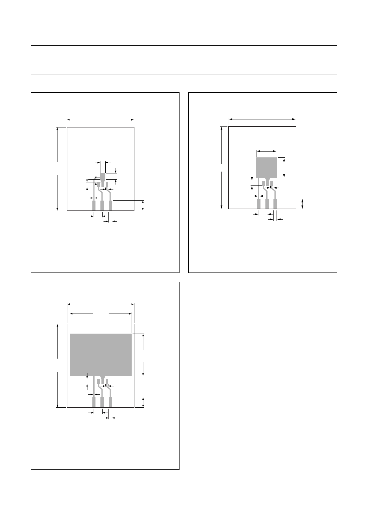
Reference mounting conditions
40
mm
2.5 mm
0.5 mm
3.96 mm
(BISS) transistor
CEsat
32 mm
2.5 mm
1 mm
3 mm
1 mm
1.6 mm
001aaa234
5 mm
handbook, halfpage
40 mm
2.5 mm
0.5 mm
3.96 mm
PBSS5540X
32 mm
10 mm
10 mm
1 mm
5 mm
1.6 mm
MLE322
Fig.14 FR4, standard footprint.
32 mm
30 mm
40
mm
2.5 mm
0.5 mm
3.96 mm
1 mm
001aaa235
Fig.15 FR4, mounting pad for collector 1 cm2.
20
mm
5 mm
1.6 mm
Fig.16 FR4, mounting pad for collector 6 cm2.
2004 Nov 04 10

Philips Semiconductors Product specification
40 V, 5 A
PBSS5540X
PNP low V
PACKAGE OUTLINE
Plastic surface mounted package; collector pad for good heat transfer; 3 leads SOT89
(BISS) transistor
CEsat
D
b
p3
B
A
123
w M
DIMENSIONS (mm are the original dimensions)
UNIT
mm
1.6
1.4
A
b
p1
0.48
0.35
b
p2
0.53
0.40
b
1.8
1.4
p3
c
0.44
0.23
E
L
b
p2
b
p1
e
1
e
0 2 4 mm
scale
D
E
e
e
1
4.6
2.6
3.0
4.4
2.4
1.5
p
H
4.25
3.75
H
E
c
L
1.2
0.8
w
p
0.13
E
OUTLINE
VERSION
SOT89 TO-243 SC-62
IEC JEDEC JEITA
REFERENCES
2004 Nov 04 11
EUROPEAN
PROJECTION
ISSUE DATE
99-09-13
04-08-03

Philips Semiconductors Product specification
40 V, 5 A
PBSS5540X
PNP low V
DATA SHEET STATUS
LEVEL
I Objective data Development This data sheet contains data from the objective specification for product
II Preliminary data Qualification This data sheet contains data from the preliminary specification.
III Product data Production This data sheet contains data from the product specification. Philips
Notes
1. Please consult the most recently issued data sheet before initiating or completing a design.
2. The product status of the device(s) described in this data sheet may have changed since this data sheet was
3. For data sheets describing multipletype numbers, the highest-level product status determines the data sheet status.
DATA SHEET
STATUS
published. The latest information is available on the Internet at URL http://www.semiconductors.philips.com.
(BISS) transistor
CEsat
(1)
PRODUCT
STATUS
(2)(3)
development. Philips Semiconductors reserves the right to change the
specification in any manner without notice.
Supplementary data will be published at a later date. Philips
Semiconductors reserves the right to change the specification without
notice, in order to improve the design and supply the best possible
product.
Semiconductors reserves the right to make changes at any time in order
to improve the design, manufacturing and supply. Relevant changes will
be communicated via a Customer Product/Process Change Notification
(CPCN).
DEFINITION
DEFINITIONS
Short-form specification The data in a short-form
specification is extracted from a full data sheet with the
same type number and title. For detailed information see
the relevant data sheet or data handbook.
Limiting values definition Limiting values given are in
accordance with the Absolute Maximum Rating System
(IEC 60134). Stress above one or more of the limiting
values may cause permanent damage to the device.
These are stress ratings only and operation of the device
attheseor at any otherconditionsabovethose given in the
Characteristics sections of the specification is not implied.
Exposure to limiting values for extended periods may
affect device reliability.
Application information Applications that are
described herein for any of these products are for
illustrative purposes only. Philips Semiconductors make
norepresentationorwarranty that such applications will be
suitable for the specified use without further testing or
modification.
DISCLAIMERS
Life support applications These products are not
designed for use in life support appliances, devices, or
systems where malfunction of these products can
reasonably be expected to result in personal injury. Philips
Semiconductorscustomersusingorselling these products
for use in such applications do so at their own risk and
agree to fully indemnify Philips Semiconductors for any
damages resulting from such application.
Right to make changes Philips Semiconductors
reserves the right to make changes in the products including circuits, standard cells, and/or software described or contained herein in order to improve design
and/or performance. Whenthe product is in fullproduction
(status ‘Production’), relevant changes will be
communicated via a Customer Product/Process Change
Notification (CPCN). Philips Semiconductors assumes no
responsibility or liability for the use of any of these
products, conveys no licence or title under any patent,
copyright, or mask work right to these products, and
makes no representations or warranties that these
products are free from patent, copyright, or mask work
right infringement, unless otherwise specified.
2004 Nov 04 12

Philips Semiconductors – a w orldwide compan y
Contact information
For additional information please visit http://www.semiconductors.philips.com. Fax: +31 40 27 24825
For sales offices addresses send e-mail to: sales.addresses@www.semiconductors.philips.com.
© Koninklijke Philips Electronics N.V. 2004
All rights are reserved. Reproduction in whole or in part is prohibited without the prior written consent of the copyright owner.
The information presented in this document does not form part of any quotation or contract, is believed to be accurate and reliable and may be changed
without notice. No liability will be accepted by the publisher for any consequence of its use. Publication thereof does not convey nor imply any license
under patent- or other industrial or intellectual property rights.
Printed in The Netherlands R75/03/pp13 Date of release: 2004 Nov 04 Document order number: 9397750 13893
SCA76
 Loading...